
One of the most fundamental challenges for computing is keeping execution units filled doing useful work. Every year, a huge portion of global computational power is wasted simply waiting for data to make it to execution cores. Aside from mechanisms such as branch predictors, speculative execution, and more that the industry employs to combat this efficiency challenge, a key component is on-chip caches. These caches keep data readily accessible to execution units.
For well over a decade, we have discussed server CPUs with cache sizes in the MB range. The Nehalem-EP parts arrived in the market around the same time as STH was founded in 2009. These chips had four cores, 8MB of L3 cache, and an IO Hub. Since then, L3 caches on Intel CPUs have generally gotten smaller, but that era is likely to change in the coming years as systems get bigger. In the not-too-distant future, we will start referring to CPU capacity stats with GB units rather than MB. We saw the first indication of this over the past few days with AMD V-Cache. As such, let us look at what is driving this, and why it will be a huge deal in the industry.
Video Version
Our video cadence has been a bit slower the past few weeks. We do have a video version of this article as well at:
As always, we suggest you open this in a new YouTube tab, browser, or app for a better viewing experience.
Next-Generation Servers with CXL
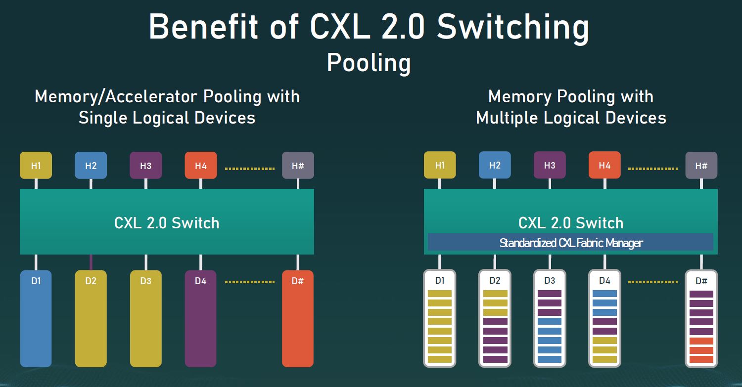
One of the biggest drivers of innovation in the server space will be Compute Express Link or CXL. The industry has discussed the idea of disaggregating compute, storage, and memory for a long time. Even this week Micron clearly showed that at its Computex 2021 Keynote vision.
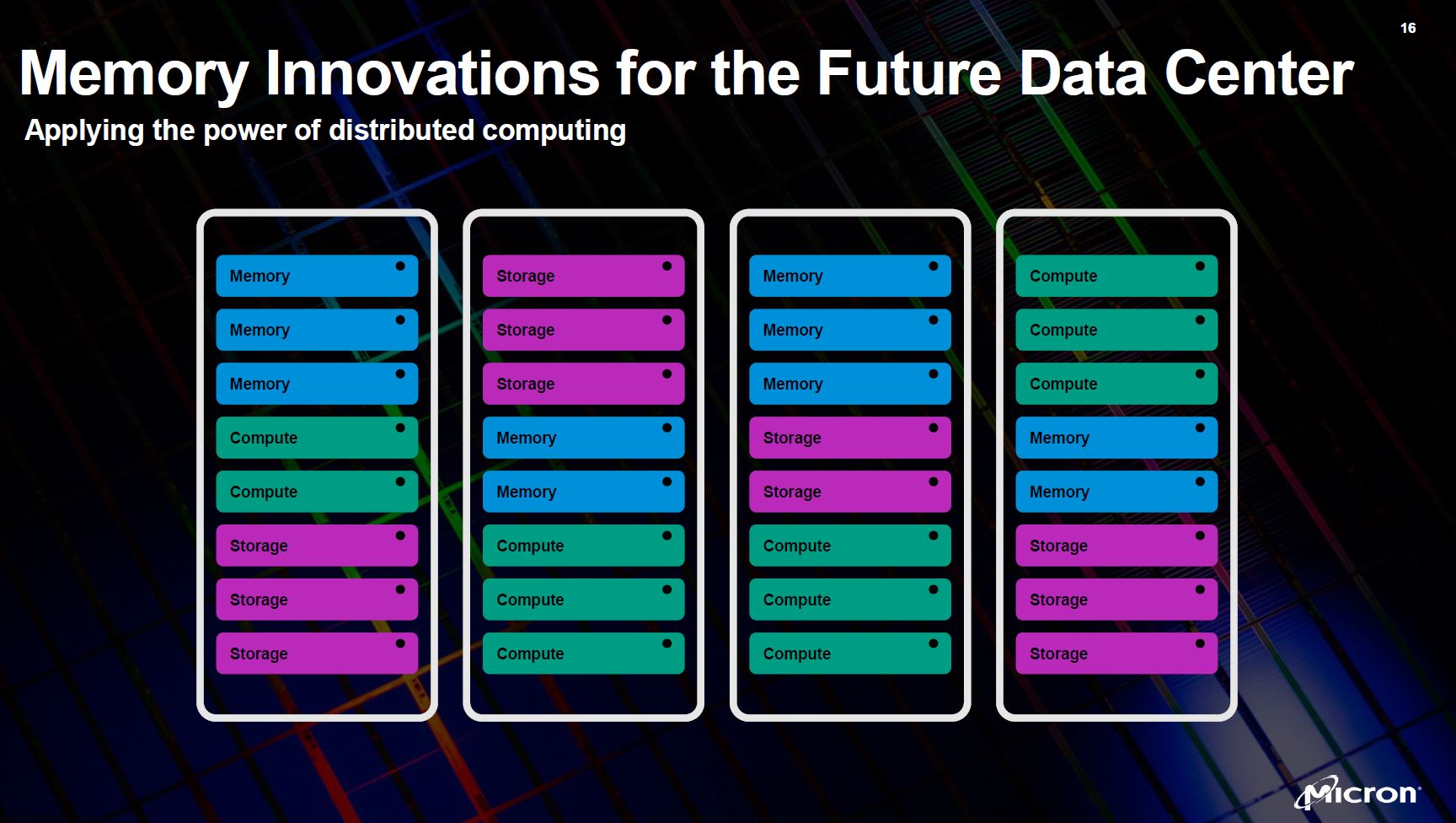
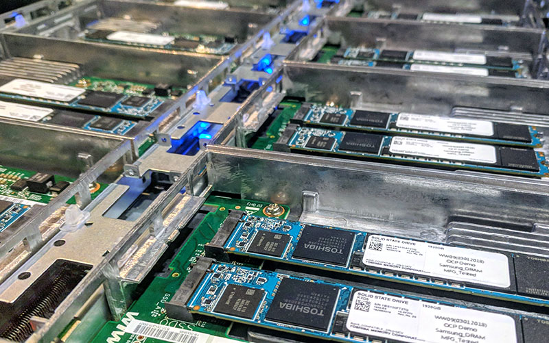
Intel and others have had similar slides over the years and this is already happening in some ways. JBOF (Just a Bunch Of Flash) chassis are common in today’s large-scale data centers. Here is an example using the OCP Lightning JBOF that we have seen thousands of in labs and data centers.
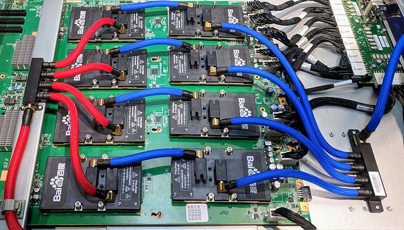
This is a step in storage disaggregation but GPUs have already been there as well moving to their own compute shelves such as this Baidu X-Man solution.
While we have seen storage and compute move into dedicated chassis, usually composable via PCIe fabrics, being stuck on PCIe Gen3 for ~9 years (Sandy Bridge-EP to Ice Lake-EP) hurt the ability to truly disaggregate as the bandwidth and latency were not sufficient for memory disaggregation.
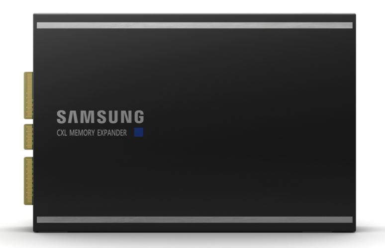
CXL will fundamentally change that paradigm. With CXL, we will get CXL Memory. Samsung already has announced its first DDR5-based CXL Memory Expander.
Effectively the same model we have had for putting storage and accelerated compute resources on the PCIe bus will extend to memory as we move to the PCIe Gen5 and CXL era. We will finally have bandwidth and latency that will help us make use of large pools of memory directly on CXL. CXL memory will be fast, but it is not going to take the place of directly attached memory in many cases just because there is a latency hit. That latency hit is something that many are perfectly willing to accept if memory capacity and utilization can go up.
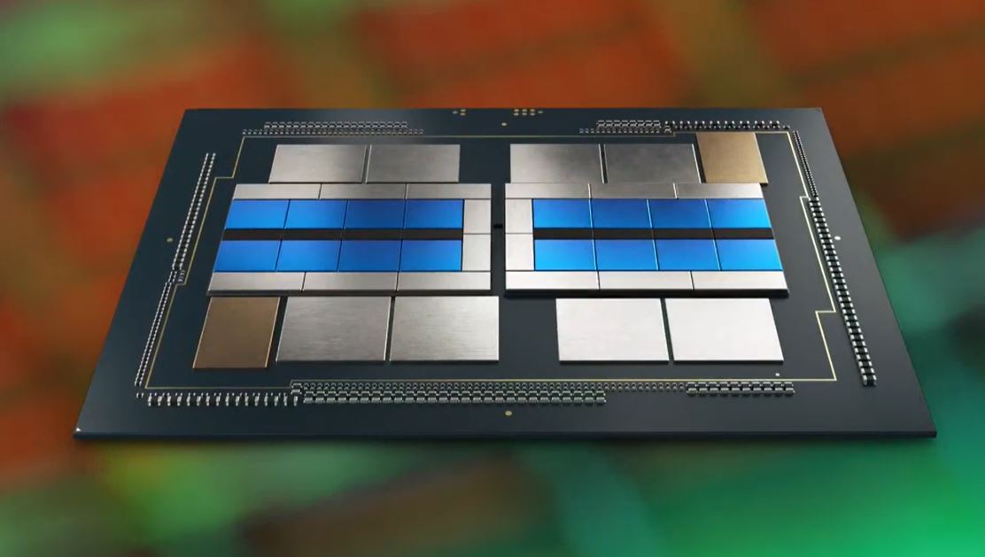
While CXL memory is one aspect, chips are also getting significantly more complex. Intel Xe HPC “Ponte Vecchio” integrates 47 pieces of silicon into a single package. One of the first features of the Xe HPC solution that Intel unveiled was the Rambo Cache. This cache is a key enabling technology of the new multi-chip design. That is very similar to how with the AMD EPYC 7002 “Rome” and EPYC 7003 “Milan” the higher cache capacities are an integral part of getting performance from a multi-chip design.
We know we are getting larger chips, enabled by chiplets in the not-too-distant future. We also know that disaggregation with CXL is happening. As such, systems are going to get better. Those two factors make it highly likely that we are going to see chips with using “GB” of onboard cache instead of “MB”. This must happen to prevent enormous costs from constantly pulling data from remote sources.
AMD V-Cache
Although Intel changed from discussing how monolithic die CPUs are better than multi-die CPUs to fully embracing its packaging advantage. AMD has been packaging multi-die CPUs for some time. Admittedly, the EPYC 7001 series was not the fanciest multi-chip CPU, but AMD is on a path. Specifically, that path is showing technology advancements with shipping generally available products. We first heard of Intel Foveros which is going into that Ponte Vecchio accelerator in the next few quarters, and there have been some other products with packaging, AMD has taken an approach that implements new packaging in products. That is what makes AMD V-Cache more interesting, AMD’s time to market is said to be in the next few months/ quarters.
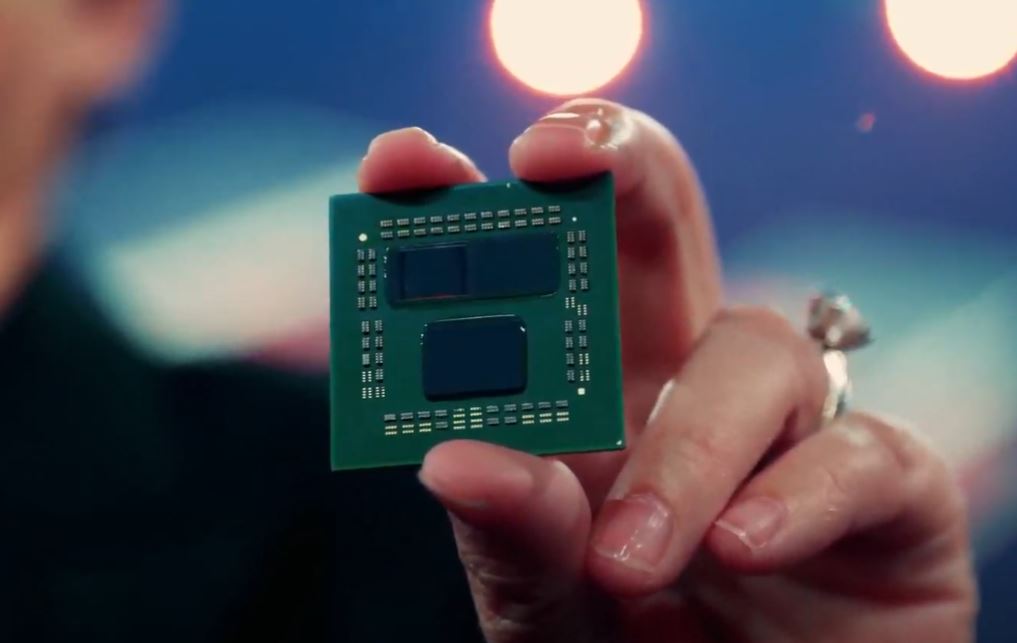
At its highest level, AMD V-Cache is a way for the company to increase the amount of cache found in its processors. The way it achieves this is by stacking a SRAM cache silicon die above a compute die. Once these two pieces of silicon are stacked, supporting structures are put in place, and a technology called Through-Silicon Via or TSV. TSV’s can conceptually be thought of as pipes to bring data and power to the additionally attached die and have been used in many products for years. As with all modern server silicon, we need data pathways and a way to get electricity to the die, which is what TSV can provide.
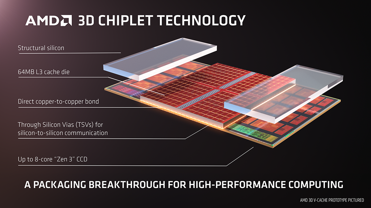
Keeping this at a high level, AMD V-Cache effectively allows the company to simply add more cache to a processor package.
Adding more cache is a big deal. There are costs in terms of power, bandwidth, and latency to transfer data across a die, from a die to another die (stacked with TSV or using another method), and to go off-package to external resources. Taking an extreme example, if one can imagine if a small record was already in a chip’s cache, then utilizing that record would be relatively low power and fast. In contrast, if that record sat in a cloud storage service, additional servers and an array of networking gear would need to be used in order to simply get the data to the chip. To a smaller scale, but on a much larger scale than on-die latencies and power, simply going to a system’s RAM to fetch data uses significantly more power, has less bandwidth, and higher latency. During that time waiting for data to be retrieved, a processor would sit idle if it were not for ingenious methods employed to extract useful efforts from the chip.
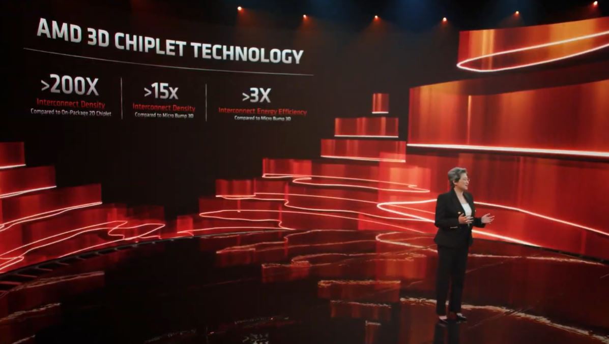
With AMD V-Cache, the impact is that AMD has a direct path to add more cache to its processors using relatively inexpensive cache chips. In the initial Computex 2021 demo, Dr. Lisa Su showed the audience how the company could stack one of these cache die devices atop a compute die from the company and triple the onboard cache capacity from 32MB to 96MB. Since she was showing a dual compute die chip, one could expect a product to have two of these TSV stacked cache die chips one for each compute die, which would raise cache from 64MB to 192MB.
Still, a Ryzen CPU is a relatively low-end part of AMD’s portfolio. While 192MB on a 16 core CPU may sound enormous by today’s standards, remember that AMD has 256MB of cache on 8 core CPUs. One can purchase a dual AMD EPYC 72F3 server and get 16 cores with 512MB or 0.5GB Of cache today, even without this technology.
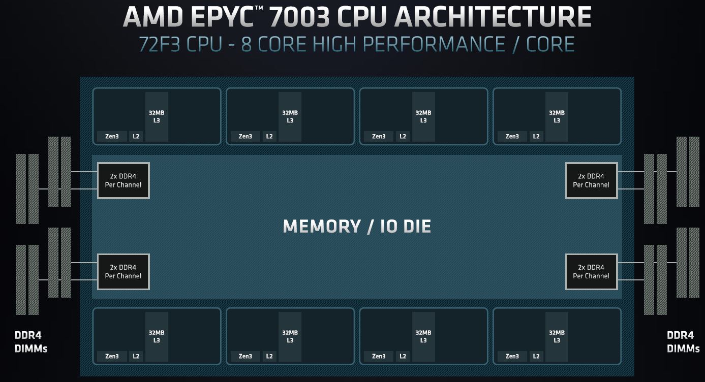
Those 8 core CPUs are constructed using eight compute dies each with a single core and 32MB of cache active. Therefore, adding 64MB of cache to each of those would mean that each processor would have 768MB of cache (or 8x (32MB + 64MB) dies.) Using this basic TSV setup in the technology demo on an AMD EPYC 7003 “Milan” generation CPU would give 768MB or 0.75GB of cache. In a hypothetical dual 8 core CPU server, AMD could deliver 2x 768MB or 1536MB/ 1.5GB of cache.
What is more, using TSV’s does not have to stop at one cache die. One can stack multiple cache dies and get more local cache. If one had 4x 64MB cache dies per compute die, then each of the eight EPYC compute dies would have 4x 64MB + 32MB of cache or 256 + 32 = 288MB of cache per die. With eight of these theoretical complexes, a single AMD EPYC would have 2304MB or 2.25GB of cache on the package.
Interestingly enough, the target market for the AMD EPYC 72F3 is per-core licensed database servers and similar applications with very high per-core licensing costs compared to the hardware costs. This is the exact market where getting more performance per core to maximize software licensing efficiency is valuable and where buyers may find 1-2GB of cache on-chip to be extremely valuable.
Looking Beyond AMD V-Cache
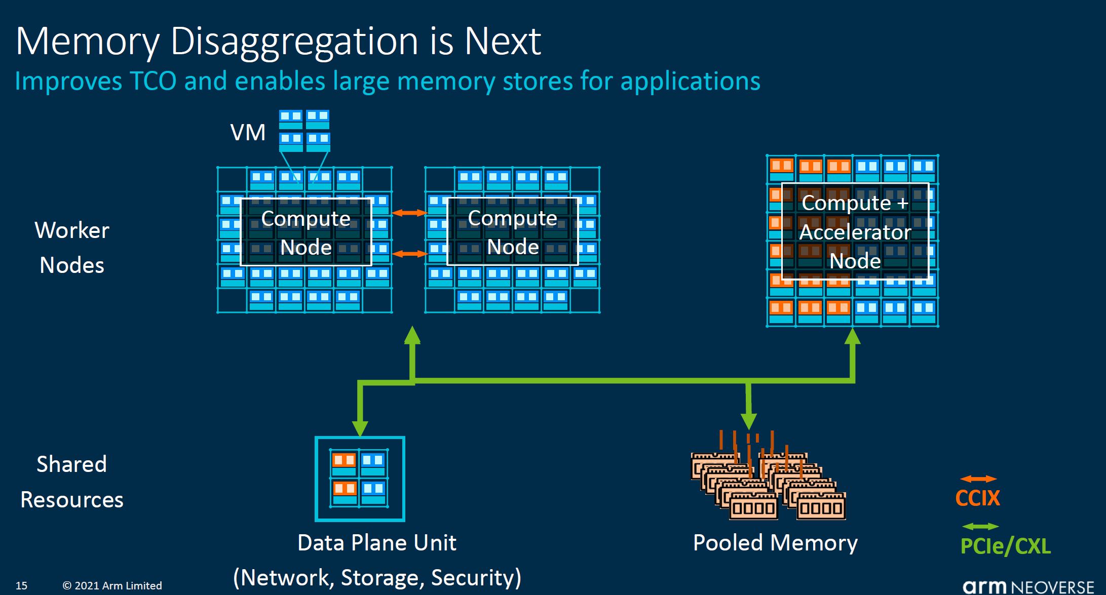
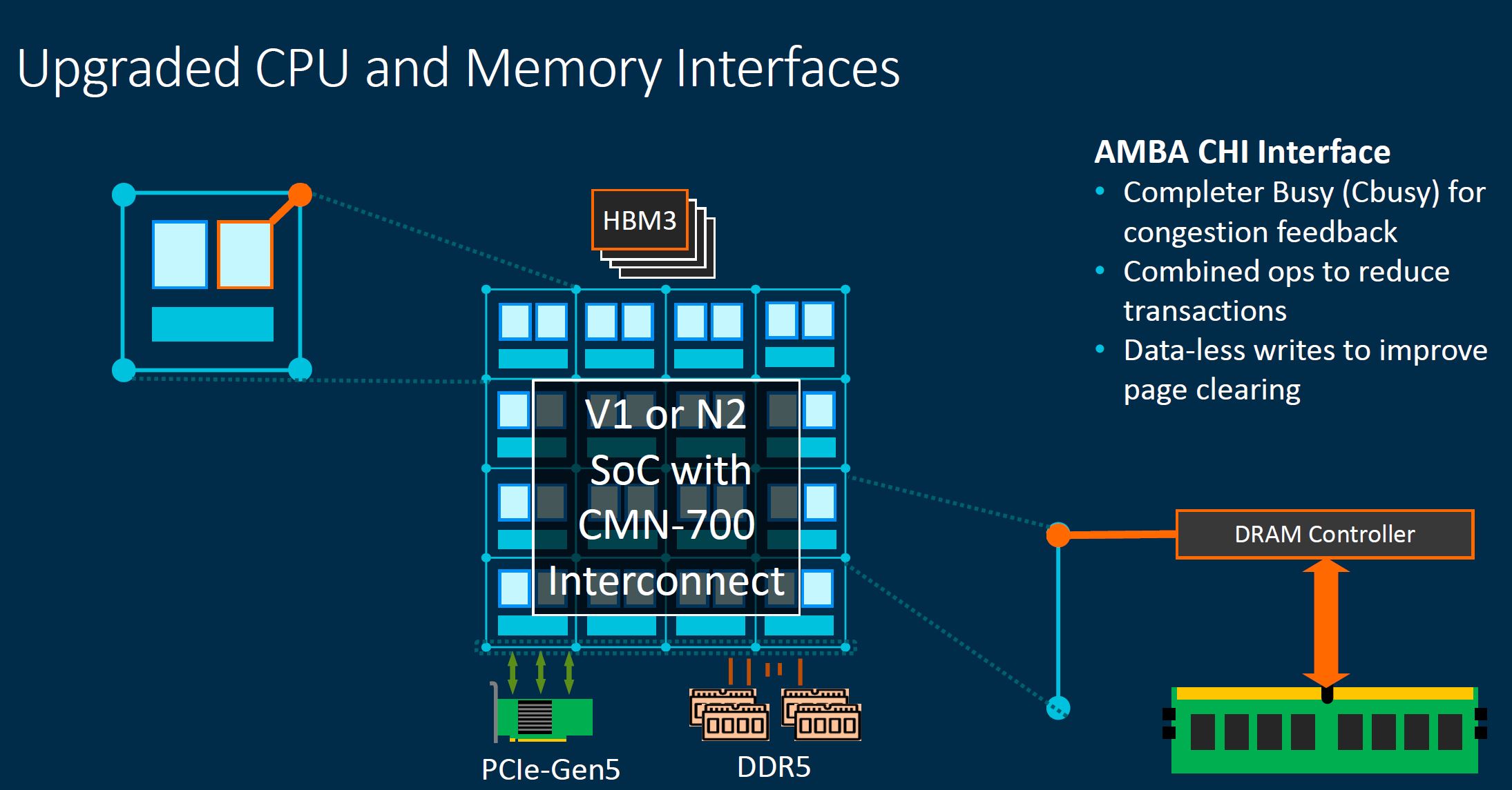
Beyond AMD, this is going to be a trend in the industry. If one recalls our overview of the Arm Neoverse N2 and V1 at Arm Tech Day 2021 many of the slides showed disaggregated compute infrastructure with pooled memory and even DPUs.
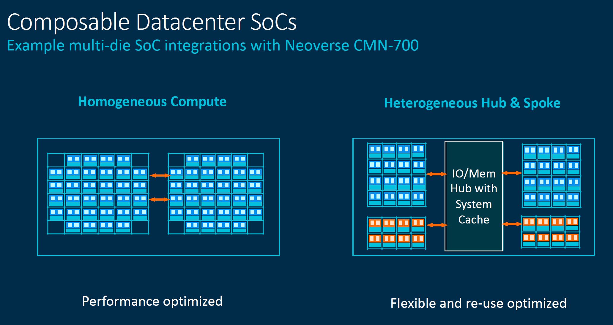
Arm was showing an I/O hub with system cache as part of its CMN-700.
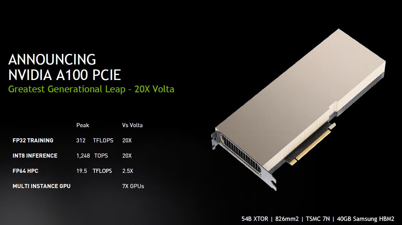
There were even Arm SoC’s mentioned with HBM3 memory. While HBM3 memory one could call more of directly attached memory, the fact that it is generally much higher performance than traditional off-package DDR memory and we refer to current chips like the NVIDIA A100 as having 40GB, means that we are likely to even discuss on-package memory in GB for future CPUs even if it is HBM not cache.
Given that in this diagram we can see a DRAM controller for off-package memory, there is a good chance that HBM in a CPU gets implemented as a faster tier than CXL or DDR system memory and perhaps becomes some sort of cache itself.
Actually, this is not too dissimilar to what Xeon Phi did years ago with its local memory able to be accessed as cache or as addressable system memory.
Intel has not officially discussed details, but when we see other vendors heading down this path towards on-chip storage being measured in GBs instead of MBs, we can imagine Intel has plans to follow the industry trend.
Looking Ahead
In a world of CXL pooled memory, multiple accelerators, and disaggregation, we are going to see larger systems. The larger topologies will often mean that components will be spread at distances and thus have more latency and more power required to access data than on-package solutions. Having more data moving through a system, and the potential for higher latency memory will push CPU designers to employ larger caches on server CPU packages. The trend is already happening and will only accelerate. As we saw 8MB per chip in 2009’s Nehalem-EP, 55MB per chip in 2016’s Broadwell-EP, and 256MB per chip in 2019’s AMD EPYC 7002 Rome series the underlying trend is fairly clear. AMD’s products have shown that having large caches helps mask some of the latency challenges from larger multi-die chips. As the rest of the industry transitions, this will be something we expect to see frequently.
History has shown the case for cache increasing by ~5x every 5 years or so, which seems to point to the prospect that we are no longer going to talk about capacities of server CPUs in MBs, but rather GBs in the near future.
The broader implication is that creating future CPUs with more I/O, more cores, additional types of larger capacity volatile memory, with many pieces of silicon integrated means that server CPUs are going to get more expensive. TCO may be better, but the incremental unit costs will most likely have to go up as well.
We have been running this recent series looking at CXL, DPUs, now CPU caches to get our readers to start preparing for future generations of servers. There is more happening here than incremental generational upgrades and the rate of change we will see over the next 1-5 years is going to be uncomfortable for those who are accustomed to the rate of innovation in the Intel Xeon E5-2600 V1 to 2nd Generation Intel Xeon Scalable eras. We have more coming on STH including a few pieces of very cool technology we cannot wait to show you. Stay tuned for more.


Wouldn’t the GB Era be defined by stacked DRAM instead of stacked SRAM
Totally may be. Stacked SRAM, DRAM, and even co-packaged HBM. The point is we are going to see a lot more onboard capacity. We just used the latest disclosures as an opportunity to show why.
@jorge
Using eDRAM or HBM certainly would bring gigabyte caches to CPUs quicker, they tend to come with the trade off of latency. Leveraging eDRAM or HBM would also need to be implemented as a separate cache level than SRAM backed caches.
This additional complexity of the cache layer would have to be compared to the latencies involved in direct attached memory and remote NUMA pools. The later scenario, caching of remote NUMA data would be advantageous even if the eDRAM/HBM latency isn’t much improved over local DRAM as main memory.
Where I see memory going is all on package eventually. With advanced MCM techniques and companies like Cerberus demonstrating wafer scale products, the amount of silicon in a single package is growing rapidly. In the end I don’t see the bandwidth or latency of external DRAM keeping up over the long term.
The future I imagine are designs where a package is filled with tiles in a checkerboard pattern between memory and compute pieces. Each memory tile has a 4-way router connected to each neighboring tile to provide immediate high speed, low latency access to a shared memory node. The memory tile contains several stacks of memory. The compute tiles are a mix of CPU, GPU, FPGA or accelerator ASICs with the potential of their own stacked caches. How much compute and memory simply becomes a factor in how many tiles get incorporated together. Ditto for memory capacity and cache.
External devices will still exist at some level but the high is going to go fully integrated on package and not look back.
But the latency penalty wouldn’t matter with stacked DRAM as you would have more cache close to the CPU, than you would have had with SRAM.
OMI is probably the path we’ll take with external memory, disconnecting memory capacity from what the socket supports.
It will soon be the data era. The storage & movement of data will be more important. The processing will be integrated with the RAM & non-volatile storage in stacks & modules. Adding, upgrading & fixing will just be like hot swapping disk drives in a RAID array. The network IO fabric between the modules is the central component not the CPU.
Depending on the workload, another level 4 cache at IO die, might be what’s coming next, eventually with another tech than SRAM, e.g. HBM.
The IO die wouldn’t have combatting heat issue with the CPU cores as the ‘current’ SRAM solution on top of ‘cpu dies’ would have, and there is generally a lot of space available on top of the IO die on the EPYC series.
The benefits would be seen best at workloads that spans across multiple CPU chiplets, where the IO die’s level 4 cache can act as a middle use cache before PCIe and memory access, and act as a shared cache among the CPU dies.
Realistically, this would at start only come to EPYC series CPU, as few workloads on client CPU’s spans across more than 8 cores atm.
However, a joker would be if AMD indeed incorporated a GPU on the IO die, because then the Level4 cache on the IO die, could act as a hybrid cache of both GPU and CPU’ chiplets, kind of like we saw with the Broadwell CPU from intel (although, limited used here).
Rather than having the large HBM as L3 or L4 cache, why wouldn’t we see designs with large HBM configured as CXL device attached memory, with asymmetric/biased coherency?
Comments are closed.