
Saying Intel Foveros is awesome is easy. For years in the chip industry, 3D die stacking has been a dream. We have seen die stacking, but never like Intel is proposing and producing. Furthermore, this is not just a concept, this is working silicon. While the Intel 10nm process node has been, let us say, slow to come to fruition, 3D die stacking leverages Intel’s packaging IP portfolio beyond EMIB. In this article, we are going to show why Intel Foveros is a big deal across a number of Intel’s verticals.
Outlining Packaging Leadership with Intel Foveros
Intel has been under a lot of pressure to deliver 10nm parts. Intel started the day with something intriguing, its packaging vision.
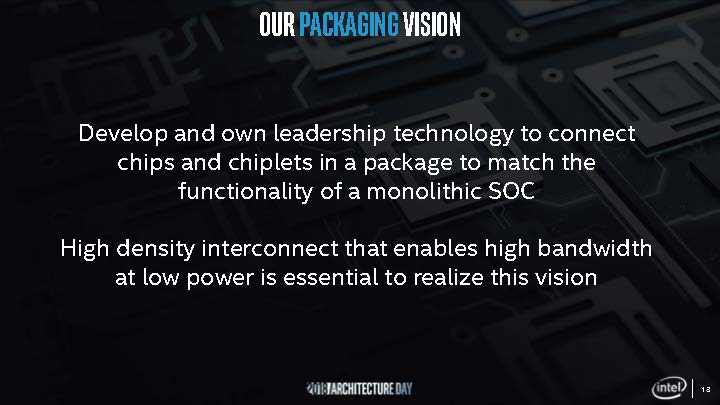
The clear implication on where chips are headed is a number of different silicon pieces sewn together with a high-speed interconnect.
Here is a chart that shows Intel’s challenge. As the company that wants to deliver the largest market share while expanding its total addressable market (TAM) it has to make many different types of transistors and circuits. The Intel Architecture Day 2018 was held at Robert Noyce’s old house. Robert Noyce was an Intel co-founder and one that filed one of the early integrated circuit patents. Jack Kirby is someone to look up, but since this is an Intel piece, rather than a TI piece, we are going to focus on that lineage. It was fun to see the transistor talk early as Intel’s heritage was making the “impossible” to build possible.
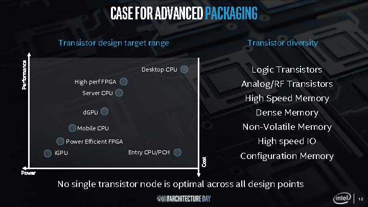
Intel’s main thrust is that all of the different transistors it makes have different cost, power, and performance requirements. Somewhat interesting in this is that a desktop CPU can cost more and does not need to optimized on power according to this chart, an inverse of the mobile CPU. Intel also has a number of processes designed for compute or I/O that are being fabbed in parallel.
Intel’s challenge was to pull together a number of discrete chips into a single package. It could optimize each chip on a given process node and then put them together in a single package.
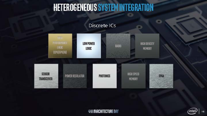
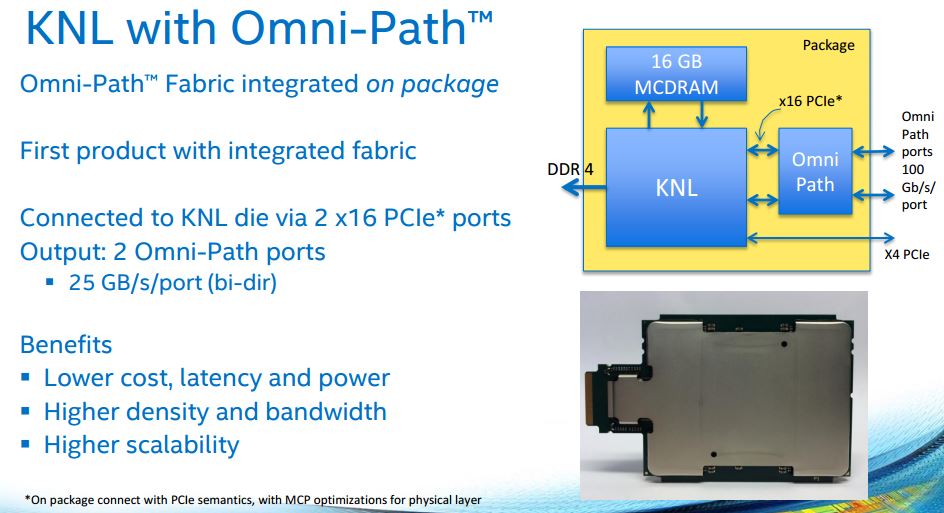
That idea is not new. Chips have been working on tieing together multiple pieces of silicon for years. While the average Skylake-SP part may be a standard package, it is designed with a low power PCIe x16 link for on-package I/O chips (Omni-Path) or co-processor chips (FPGA.) Knights Landing was a bit different as it had not just the CPU onboard, but also Omni-Path and high-speed MCDRAM. You can read a bit more about that MCDRAM in our Supermicro SYS-5038K-I-ES1 Intel Xeon Phi x200 Developer Workstation Review. Intel has been doing multi-chip on-package for years. You can even go back to the Pentium II era (circa 1999) and Intel was mixing die on a single package with off-chip cache and the main CPU.
EMIB is what, until this week, most in the industry thought Intel would use for multi-chip. High density, high-speed, chip-to-chip interconnects sounded great. Put chips together like a Scrabble board and you can build packages from a number of chips that can act like they are on a single piece of silicon.
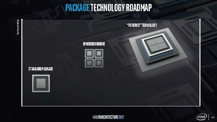
Then Intel Foveros came along and changed that viewpoint. Intel is stacking chips not just side by side like Scrabble but is building chips like Legos.
Next, we are going to get onto the implications and the actual demo, but before we do, here is a bit of STH bonus fact check trivia for our readers.
Bonus Trivia: Foveros in Google Translate
At STH, we strive to give our readers something to talk about around the water cooler at work. Here is a fun one you can do. Using Google Translate (via the normal search box) and translating foveros from Greek to English you get fearful with Awesome as an adjective:

I do not think that is what Intel was going for with the translation, however, it is all Greek to me. If you add Intel in front of foveros, you get Intel Awesome:

If instead, you use the formal Google Translate, and not the search bar version, you get this:

10nm challenges, Intel Foveros, or “do not worry.” That seems to be one of the key messages from Intel Architecture Day 2018.
I am sure our readers can think of more clever ways to use this with their co-workers.
Now onto more about the technology.


I’m loving that there’s an ounce of personality in STH nowadays. Now 10nm just needs yields.
Oh and intel foveros you can have a foveros day.
How is Intel handling the cooling when IC’s are stacked like LEGO?
Does Intel license what it call “AMD Glue” to glue chips together? :-D :-D :-D
Intel Inside = Spec Violations Inside – Kernel Relocation Inside = $$$ for Intel Inside!
It’s so amazing people, especially IT, have been not only accepting but also enjoying paying more for the faulty products!
Complete guess here, but thermal capacity of these chips has to be tiny… A much smaller surface area for thermal dissipation (look at how big that heatsink is on the demo vs the chip size itself) and the thickness will lead to catastrophic heatsoak in a short time. This process, although intriguing, still must be flattened out for thermal purposes or stay limited to super low power uses, looking at thin/zero clients and such that can still house a decent heatsink. The issue with modern portable devices is heat throttling, and I see this being even worse for those.
Liquid cooled laptop anyone?
Well, as a Greek I can clarify that foveros means awesome in this context. The main issue with this technology is the heat dissipation and also the limit of the pin count because of the smaller area (depending what they want to achieve).
Comments are closed.