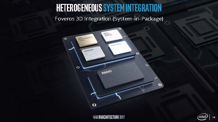
Intel Foveros Technology for 3D Packaging
Intel Foveros was introduced as a way to tie a number of different chips and chiplets from different processes together into a single package to match the functionality of a monolithic SoC. It uses a high density interconnect that enables high bandwidth at low power and is essential for that vision. Intel’s first step, EMIB, was a play to achieve around 5x density and 1/5th the power. With Foveros, bump density is at least 50% better and is lower power as well. The reason we are not seeing more EMIB used more broadly is that Intel Foveros came along and presented something superior. Again, this is Legos, not Scrabble.
Part of the challenge with the co-packaging of heterogeneous die is that each die has different external connection needs. Just to illustrate what this looks like at the package level, here are your three main dual socket server CPU options today, and the connections they require:
To conceptualize what this challenge entails, think about how to get these chips to talk together and to the rest of the platform. The Intel Xeon chip to the right uses a Lewisburg PCH while the other two do not use a PCH. Also, each of these chips has different power requirements and different thermal cooling requirements.
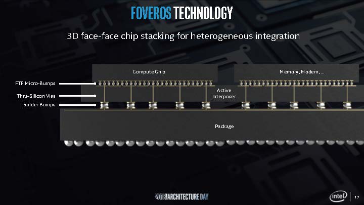
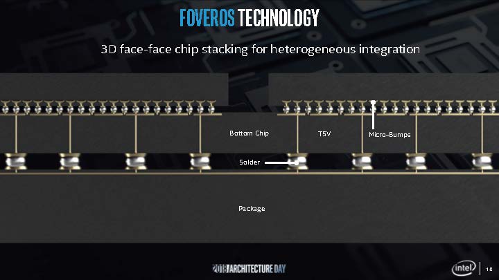
Intel Foveros uses high-density bumps along with Thru-Silicon Vias and an active interposer to facilitate this communication.
Intel said there have been a number of papers on this type of technology, but production introduction has been a different story. One has to figure out the thermals of putting chips together. Power delivery through the design is not easy since it is passing through multiple layers and that has its own design challenges. Also, how do you do know during the process that you are using a known good die? Assemblies get expensive when one part does not work and breaks the rest of the chip. Finally, how do you make 3D die stacking a high-volume manufacturing possibility? Intel Foveros is the company’s answer saying that the company has the R&D grunt and packaging prowess to work through the challenges.
If you are thinking, that this sounds like what AMD and NVIDIA are doing, let us take a second and look at the differences.
AMD Rome and NVIDIA Tesla v. Intel Foveros
One may say, different chip types, using different fabrication process nodes, combined into a single package, that sounds like AMD EPYC Rome (or Naples) or NVIDIA Tesla. It is not the Faveros approach and the difference is compelling.
AMD is mixing chiplets with Rome but in a very different way. It is using a PCB interconnect. AMD needed to keep the I/O logic on 14nm while it is moving its CPU logic to 7nm. I/O is harder to shrink and that is why we are seeing Intel also talk about using different process generations for I/O versus compute logic.
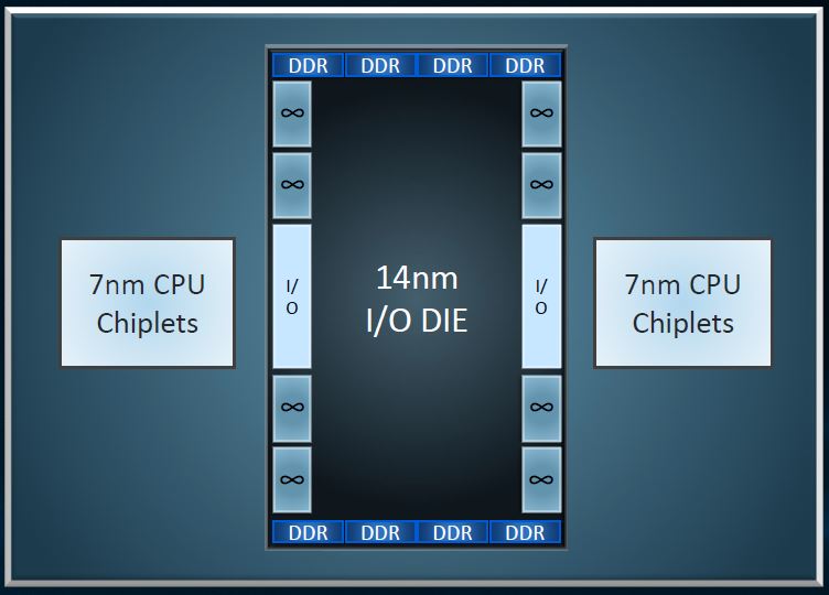
Intel also said I/O and compute can and perhaps should be on different pieces of silicon.
NVIDIA uses CoWoS on its high-end Tesla GPU packages to connect its GPUs to high-speed HBM2 memory. Here are a few chips from our DeepLearning12 build where you can see four HBM2 die and a GPU die on another piece of silicon between the five chips.
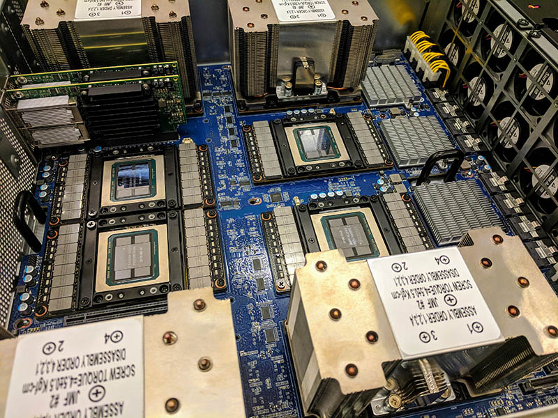
That uses a much simpler interposer than Intel is using and is very fragile. STH now owns a $350 screwdriver because of how fragile this setup is. (Read more about that in How to Install NVIDIA Tesla SXM2 GPUs in DeepLearning12.)
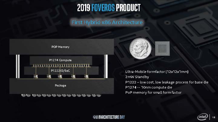
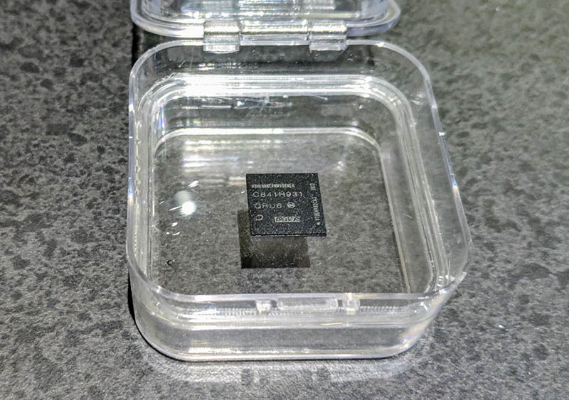
The Intel Foveros Chip Gen1
When asked if this was simply a tech demo, Intel said no. This will be a shipping product on its parts list for 2019. Indeed, Intel went one step further and showed off its first Foveros product. Outlined in the presentation was a 12mm x 12mm package with memory and two different compute and I/O chips. One chip was using 10nm and one was a lower leakage 22nm process part for the I/O and SoC chip.
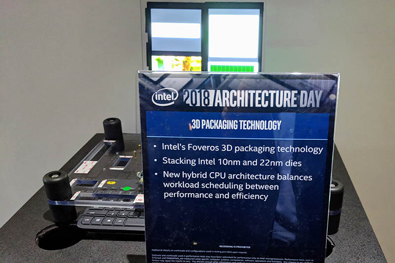
Slides are great, Intel had this shown off in the family room of Robert Noyce’s former home.
The chip itself is very small and designed for ultra mobile applications. When asked how much this chip costs, we were told by someone holding the chip, “more than my life” which we felt was more of a statement around the high value of such a cutting-edge engineering part rather than a way to downplay the individual’s self-worth.
The implications of such a small part are more than just combining a 22nm part (Intel is very good at 22nm) and a 10nm (Intel has lower yields on 10nm) chip. Putting memory, I/O, and compute onto a single platform means fewer motherboard components. There are fewer wires for the motherboard as well to connect discrete chips. Just for comparison, this single chip is smaller than your average AST2400/ AST2500 chip. Here is an ASPEED AST2400 example from our ASUS RS520-E8-RS8 2U Server Review.
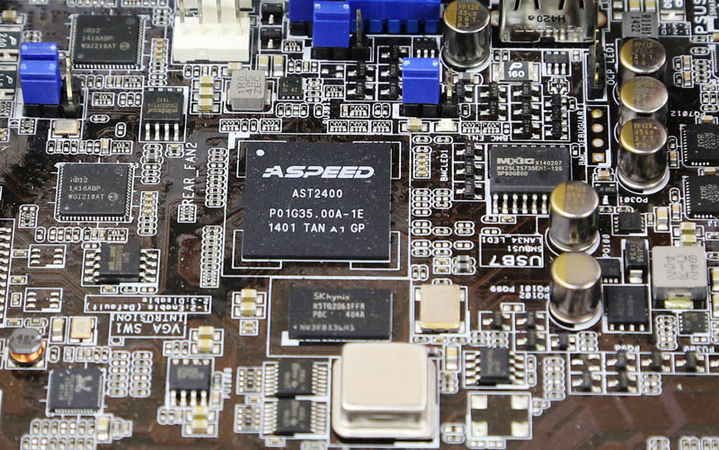
You can see the main SoC. Below that you can see the SK.Hynix DRAM. You can see the flash memory chip for the embedded OS. You can also see on the bottom left here the Realtek NIC that is used for its management ethernet. Look at how far apart those components are, and how much PCB room they use. You can see traces running between them. On a server motherboard, this is the easy part. On a mobile device like a thin laptop, less motherboard spaces means a bigger battery. Integration is king and Intel Foveros enables that on its first 12mm part.
Intel not only had a chip on display, but it had Foveros running in a “hey guys look this works” moment.
This is not just slideware or a completely future technology. This is something working in 2018 destined for products with a real benefit in 2019.
Final Words and the So What
For now, Intel can make some fairly large 14nm and 22nm chips. It has years of experience on those processes. 10nm is more of a challenge. As much as Intel downplays the challenge, it is still there. Using Intel Foveros the company can prioritize getting yield from the parts that will most benefit from 10nm and cost-optimize the rest away. That, in turn, makes simpler and smaller 10nm parts while enabling smaller footprints and simpler motherboards by stacking die atop of each other. In theory, Intel could make a multi-die server part from this as well. One of the other intriguing parts here is that Intel can also make a multi-die solution for the data center not just with x86 compute and I/O, but also with FPGAs, NNPs, and GPUs. I am not sure what the GPU part of an Intel Foveros x86 comptue die with a GPU die would be called. iGPU since it is integrated? dGPU since it is a distinct chip? fGPU because it is a distinct chip using Intel Foveros? Please let it be fGPU.
The implication in the mobile space is going to be the first step. For the data center, managing high TDP chips and their power needs is a bigger challenge. At the same time, the data center is where Intel makes its biggest monolithic chips today and where it will see a big benefit to moving to multiple die. Intel Cascade Lake-AP is going to be multi-chip but we do not expect it will be Foveros at this time, and even Cooper Lake may be early for Foveros in the data center. Make no mistake, Intel needs to go multi-chip in the data center in the next few years so a denser, better performing, and lower power way to stich together chips is extremely important for our readers.


I’m loving that there’s an ounce of personality in STH nowadays. Now 10nm just needs yields.
Oh and intel foveros you can have a foveros day.
How is Intel handling the cooling when IC’s are stacked like LEGO?
Does Intel license what it call “AMD Glue” to glue chips together? :-D :-D :-D
Intel Inside = Spec Violations Inside – Kernel Relocation Inside = $$$ for Intel Inside!
It’s so amazing people, especially IT, have been not only accepting but also enjoying paying more for the faulty products!
Complete guess here, but thermal capacity of these chips has to be tiny… A much smaller surface area for thermal dissipation (look at how big that heatsink is on the demo vs the chip size itself) and the thickness will lead to catastrophic heatsoak in a short time. This process, although intriguing, still must be flattened out for thermal purposes or stay limited to super low power uses, looking at thin/zero clients and such that can still house a decent heatsink. The issue with modern portable devices is heat throttling, and I see this being even worse for those.
Liquid cooled laptop anyone?
Well, as a Greek I can clarify that foveros means awesome in this context. The main issue with this technology is the heat dissipation and also the limit of the pin count because of the smaller area (depending what they want to achieve).
Comments are closed.