
Between events at AMD Next Horizon event in San Francisco, I wanted to do a quick recap of the new AMD EPYC 2 “Rome” platform. There were a number of disclosures today, and we can now have a discussion on what the next-generation performance picture will look like. You can see our AMD EPYC 2 Rome at the Next Horizon Event coverage to learn more.
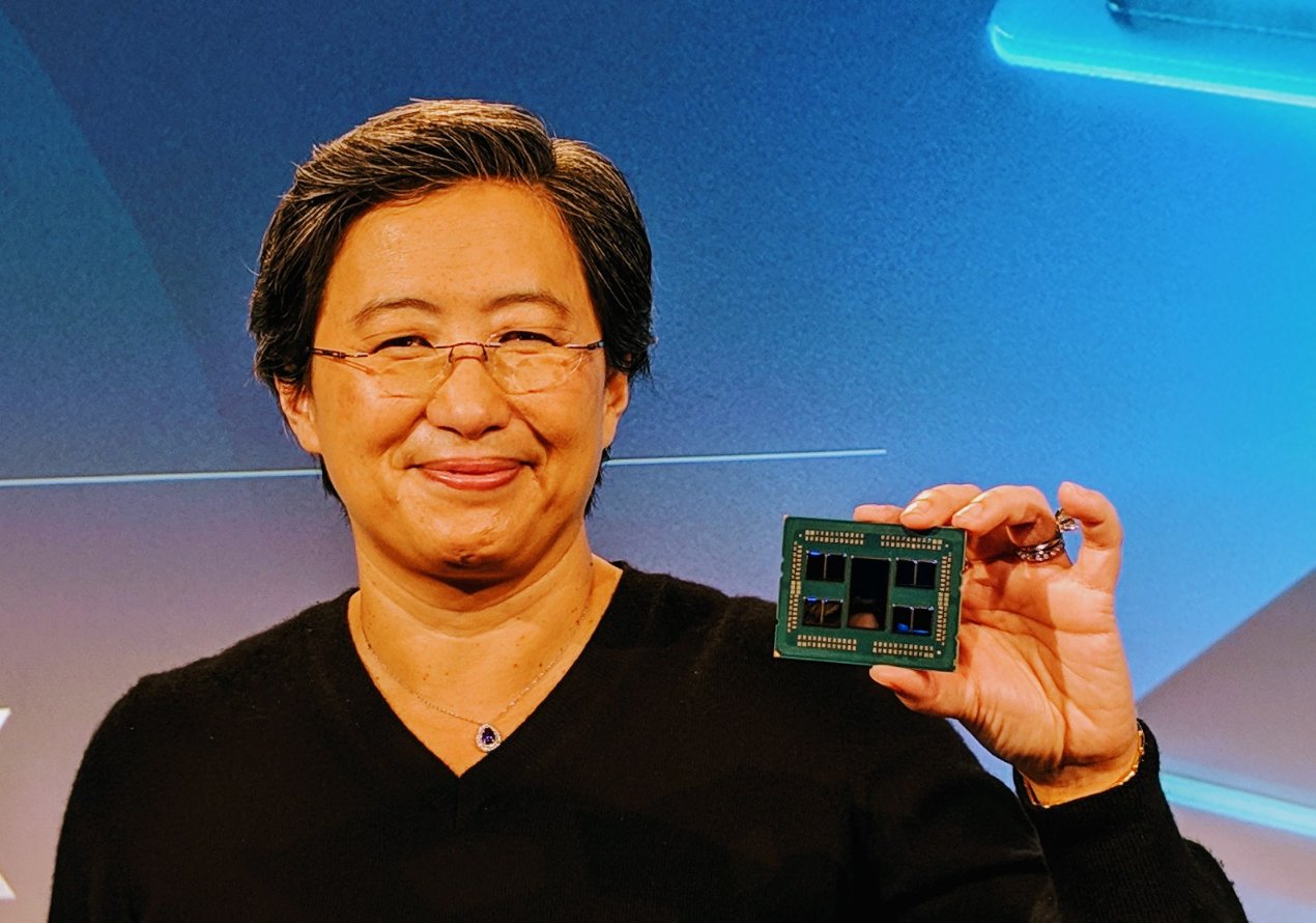
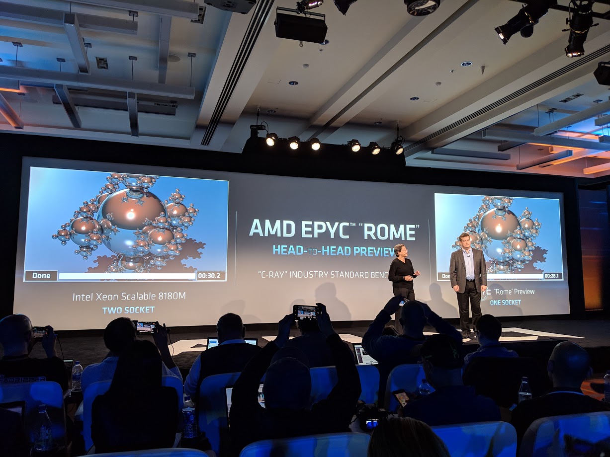
The star of the show was the new AMD EPYC 2, here it is live with a triumphant Dr. Lisa Su, CEO of AMD:
AMD EPYC 2 Rome Details
Here is the quick summary of what we learned today about the AMD EPYC 2 “Rome” generation:
- Up to eight 7nm x86 compute chiplets per socket.
- Each x86 chiplet up to 8 cores
- 64 cores confirmed AMD EPYC Rome Details Trickle Out 64 Cores 128 Threads Per Socket
- There is a 14nm I/O chip in the middle of each package
- This I/O chip will handle DDR4, Infinity Fabric, PCIe and other I/O
- PCIe Gen4 support providing twice the bandwidth of PCIe Gen3
- Greatly improved Infinity Fabric speeds to be able to handle the new I/O chip infrastructure including memory access over Infinity Fabric
- Ability to connect GPUs and do inter-GPU communication over the I/O chip and Infinity Fabric protocol so that one does not need PCIe switches or NVLink switches for chips on the same CPU. We covered the current challenges in: How Intel Xeon Changes Impacted Single Root Deep Learning Servers. This can be a game changer for GPU and FPGA accelerator systems.
- Socket compatible with current-generation AMD EPYC “Naples” platforms.
- Although not confirmed by AMD, we will state that most if not all systems will need a PCB re-spin to handle PCIe Gen4 signaling. So existing systems can get Rome with PCIe Gen3 but will require higher-quality PCB for PCIe Gen4.
- Claimed significant IPC improvements and twice the floating point performance per core.
- Incrementally improved security per core including new Spectre mitigations
This is a long list. We now have a fairly good idea about what the next-generation will offer. Cache sizes, fabric latencies, clock speeds, I/O chip performance, DDR4 speeds and other aspects have not been disclosed, so there is still a long way to go until we have a full picture. We have heard rumors of, and AMD hinted at the notion that with 7nm they would be able to get increased clock speeds as well.
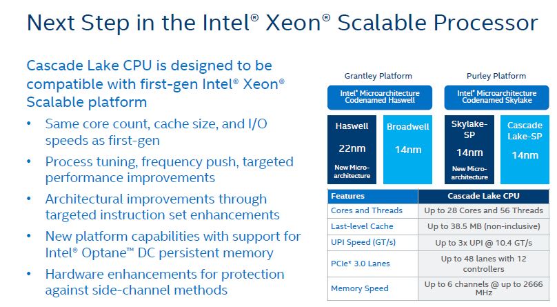
As a reminder, here is the Intel Xeon Scalable “Cascade Lake-SP” overview:
With this information on both sides, let us do a quick comparison regarding what we know at this juncture based on the disclosures each company has made.
AMD EPYC 2 Rome v. Intel Xeon Scalable Cascade Lake-SP
We are going to focus on the Intel Xeon Scalable Cascade Lake-SP segment, not the recently announced -AP parts for reasons we will get to later in this article. For now, here is a tally of where we are:
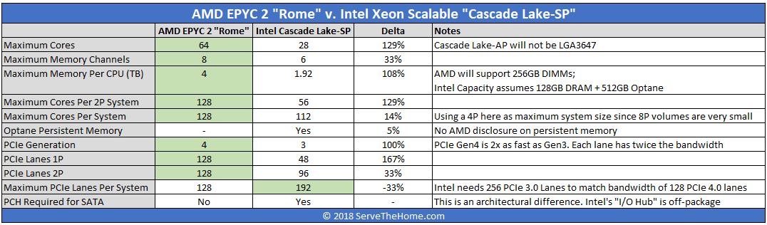
There are a few major points here. First, AMD EPYC 2 Rome stacks up closer to a four socket Intel Xeon Scalable server. Even in many of those cases, AMD EPYC 2 Rome still has several points where it comes ahead. Intel will have Optane Persistent Memory and features like VNNI for inferencing. As we wrote in our Hot Chips 30 piece’s closing comments Intel needs more. These are technologies that are first generation parts that may become important in the future, but it will be some time before there is broad enough support to say that virtually every server will use both features every day.
We also wanted to note, the idea of an I/O hub is not new. If you go way back to the 2011 ServeTheHome archives, you can see evidence in our Supermicro X8DTH-6F Motherboard Review Dual IOH to see that dual I/O hubs were a feature. Intel still has a number of Lewisburg PCH options. That is important because it means the cost of an Intel platform also needs to include the PCH. The platform TDP is an extra 15W or more due to this PCH and costs $57 or more in trays. Unlike the northbridge/ southbridge setups of old, modern Intel platforms terminate PCIe (except for PCH PCIe lanes) and DDR4 on the CPU package, but Intel absolutely still has an I/O hub in their architecture, just sitting off-package on the motherboard.
What About Intel Cascade Lake-AP?
Intel wanted to get ahead of the news and offer its own solution, the Intel Cascade Lake-AP. Intel has entered the multi-chip package arena with this announcement. As we described covering that piece, it is truly interesting.
At the same time, there are some huge differences. First, Intel Cascade Lake-AP will almost certainly require a new socket. That means if you have standardized on the Dell EMC PowerEdge R740xd you can use Cascade Lake-SP in your mid-2019 server buys, but not Cascade Lake-AP. We have not heard broad vendor support for this, and so one option is that Intel could produce PCB with the Cascade Lake-AP chips attached and offer it directly. This is not something we can see mainstream server vendors pushing to their customers.
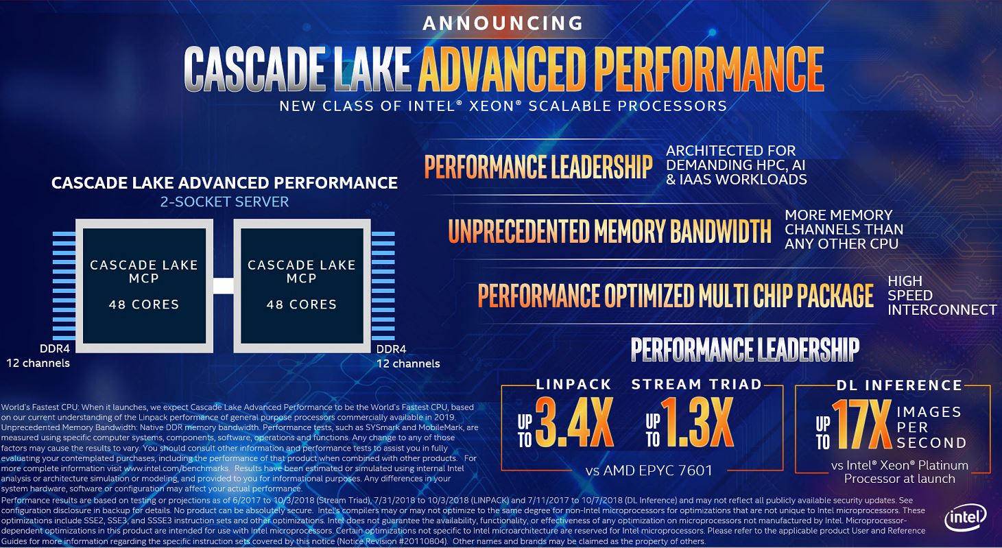
Intel offered the chips, but it did not offer a roadmap for the platform. As it stands, Intel’s announcement of Cascade Lake-AP is a one-off product until Cooper/ Ice Lake arrive. That is important for customer buy-in. Customers generally do not like single generation products.
In many ways, the Cascade Lake-AP dual socket architecture looks like a quad socket Intel Xeon Scalable system, just in two packages. As a result, the numbers should be close to the above 4P numbers, except with an asterisk that Intel may be able to get up to 256 PCIe lanes from their platform. That would give more lanes to Cascade Lake-AP and bring bandwidth parity with Rome.
Until we learn more, we are not going to assume this is a mainstream product.
Final Words
AMD knows it has a monster chip with the AMD EPYC 2 Rome generation. All of the system vendors that we talk to know that Rome is going to be big. We have seen server PMs get almost giddy as they discussed the platform.
On one hand, Intel is going to lose the top performing mainstream x86 architecture crown in 2019 by a substantial margin. At Hot Chips 30, we were told that the Intel Cascade Lake-SP specs would not change from what was presented. One can argue with the current Naples generation NUMA architecture and cores that Intel Xeon is faster. At the same time, so long as Rome’s I/O hub is reasonably implemented and performant, it will not be a close race as we start the second half of 2019. Intel may retain the per-core performance lead which is important for many licensed software packages. In terms of total performance, Intel is going to be behind.
The bigger question is whether this will matter. Looking forward to Zen 3, assuming that is socket compatible with the current generation AMD EPYC SP3 platforms, that is a big deal itself as it gives Intel a generation to catch up or leapfrog AMD with a newer/ bigger platform. Beyond that, AMD still needs to sell chips. AMD still does not have 10% of the market, let alone 5%. Rome will be a monster design, but the enterprise market is slow to move.
We will say this: if you are a VMware organization looking for hyper-converged setups to run Linux VMs, Rome will present a borderline obscene value especially when paired with 100/200Gbps networking and PCIe Gen4 NVMe SSDs.
The next year or two in the data center is going to be really fun. Stay tuned to STH as we cover this exciting space.


Will Asrock Epycd8-2T motherboard be shipping before Epyc2 ships??
correction: on delta for PCIe 4 vs 3 .. it should be either 100% or NA perhaps … not 33% (diff between 4&3).
I was quite suprised to see that IO chip in middle… interesting design choice. i guess it will increase latency a bit ..but will be more consistent. Although i am more interested to find out how it will impact the frequency of those chiplets..actual cores… since IO is out into another chip….cores might be able to Turbo better..or even have higher base frequency.
Yeah, i want to see more latency figures, thats the main issue with EPYC (for my workload), they are great at alot of workloads but with workloads that rely heavily on low latency AMD is far away from beating what Intel has to offer.
I really would like to see AMD lower the latency of their design, once they achieve that then they will truly have an architecture that can replace Xeon:s in all workloads
“Intel may retain the per-core performance lead which is important for many licensed software packages.”
I don’t think all EPYC 2 CPU’s will have 8 (relative)slow cpu dies, some will have 4 or even 2 very high speed dies hence 4 GHz+ speeds and still be in the thermal envelope.
PCIe is twice as fast, is the same valid for infinity fabric?
The first impression is pretty good.
“Rome will be a monster design, but the enterprise market is slow to move” While perhaps true, nearly half the market these days is ‘cloud’ who are not slow to move. AMD getting a few large design wins among that lot is sufficient to rapidly move the needle into 10%+ area over the course of 2019. Traditional enterprise may well be a lumbering beast and more amenable to kickbacks from Intel, I doubt the same can be said of 7+1
Misha, are you sure about 2 high-speed dies / 4 GHz+ speed on Epyc 2? Do you have any insider info/leak for this? I’m curious since having speedy Epyc would be better than TR due to more RAM flexibility. Thanks!
@Author,
With 7nm, 0.5x the power and 2x the density (core count), so 2x the performance with 1x the power per package.
2x the performance per watt (from 7nm), but 1x the IPC performance with all the architecture improvements?
@KarelG
When all the I/O is done by the 14nm I/O die, they have freedom of choice.
I have no inside info or leaks, but it does make sense to me when they would go that way.
David, I am going to give you another thought on this one. They need 8x (significantly) higher-speed Infinity Fabric links on the new chips. They are also adding PCIe Gen4. Doing interconnects is not a low-power affair. Think of the NVIDIA DGX-2 that uses over 3kW by adding the NVSwitches and the PHYs.
Gen1 v. Gen2 EPYC is not just about the 7nm x86 chiplets. The real story will be how AMD is managing the power on 9x pieces of silicon with a high-speed fabric between them.
Also, the I/O Hub will use a significant part of the power budget but it will bring device to device PCIe signaling without using PCIe switches at PCIe Gen4 speeds.
64 cores is impressive, but thinking of it beyond raw compute and in terms of overall platform performance is where I expect the big story to be. AMD is at 2x the core density over the previous generation which is a huge deal. 512/ cores 1024 threads in 2U with faster NVMe storage and 100GbE/ 200GbE networking
I think they have an amazon cloud deal already. Check out the new m5a instances they are Epyc based
Just had confirmation(Scott Aylor of AMD) on high frequency low core count while maintaning the rest of EPYC ROME’s strengtth (octa channel mem, 128 PCIe-4 lanes, etc…)
I had a drink with Scott last evening along with Ian Cutress, Paul Alcorn, and Charlie Demerjian.
There are going to be things coming out between now and Rome. Sit tight.
I am stunned by the GPU fabric capability.
This has just caused me to cry out Bingo! for a game that I didn’t know I was playing:
I realized this would be a terrible hypothetical waste of capabilities, but the architecture that I most desire, which has only leapt into my mind upon comprehension of the most immediate details, is:
16 cores+ of maximum L2 cache, *consistency* of turbo clock of my greatest interest,
PCIE4 to enable switching capacity for small clusters
(I am speaking out of turn, but the appearance of optical interfaces with real proximity to, if not integration with the CPU package, I believe will be the mark at which a significant input to the exponential growth hockey stick entrance*, I have been thinking about how Intel could be more confident than we are, about the nearing future,see below)
Fabric for a”tray” or horizontal card for MXM GPU units.
Generalized bus routes, direct and switching, to cope with Optane DIMMs and everything under the sun. But I will be pursuing my interest in how Optane Squared, is handled by different architecture. I am wondering, what feeds the Optane DIMMs? I will want to test, soonest possible, naturally. We are extremely space and power constrained. I am wondering, if Optane expansion cards, on switched busses, when used to buffer DIMMs , will suffer greatly, in my application case, where the buffer is feeding fresh data for indexing, that’s random. The availabilitiy to begin indexing is a internal benchmark, and we’re required to be dumb about the data structure. I am hopeful that the switching latency and shared channels, will be tolerable, because the design is aiming to load up to two jobs simultaneously, to permit CPU upgrade, hoping that the new process will bring more cores with huge L2, but expecting to wait for the first 8 core new big L2, and longer for 16 cores; Intel may still be behind for equivalents even in current generation, and being a I/O targeted processor, core count may not be demanded before clock speed and the new busses. 16/32, 4+GHz, 160MB L2 would be nothing less than the transformation of our entire business.
I totally fixed up my comment on the follow up, then ran headlong into my work, which I best should be not diving into just yet. But we have, from one view, the great niche market storage converged infrastructure application, if only the storage world didn’t pass over the big cache, high clock and low core count SKUs the kind that we are inseparable from.
I am afraid that the idea of a sixteen core, top clock and max cache chip with PCIEv4, totally threw me, earlier. Having had a chat here, I will say generally the reason is that we can then ship workstation type boxes, capable of delivering our business stack on the user’s desk. Uf I said that we develop a glorified image metadata and picture editor (the kind who chooses the portrait for the front cover of SI, eg) solution, I guess I would not be too wrong to imagine the reader blinking and preparing to type in something like, “I suppose your app is emulating the last decent System 7 version of ACDSee, in WebASM, Electron and you ported that java object database, with binary emulations in case it crashes upon indexes containing the words, “run, one, anywhere, and write”. The only thing you would be right about, is the fact that lots of great technology got washed away when the Web came along, and I can only say that you can’t build foundations starting out on the forty second floor. Maybe you can do that with a game, but, “maybe…a game” must date me… I will leave it at, just see what the biggest names without challenge, in the history of Microsoft, wrote as their swan song, coming back from retirement to do so. Not fixes but ground floor works.
I must return if I can add anything later, but for about a year, I have exhorted anyone who is young and unlucky enough to make time for me, to regard this period as a unimaginable opportunity for a career in computing. Enough is changing, I myself have been feeling that it’s a new fresh start over. I am responsible for a twenty three years old project, that I think will soon be a desktop demo, from a aisle of racks to begin, which were hardly delivering the usability of today. User interfaces with small supers not being desperately convenient. This is as significant as the Carnegie Mellon prediction of”3M” workstations; megapixel, megabyte RAM, megahertz processing, which I have etched in my mind, growing up anticipation of the day of that breakthrough. I defined my life by dropping out to enter business to be able to get my hands on the reality. STH to me, is only superficially about servers. I look here, to see the prospects of tomorrow’s workstation. I think this website will be notable indeed, in future eyes clearly seeing far greater significance.
I’m interested in the GMI links to Vega. Doesn’t this give AMD it’s own higher bandwidth version of NVLink on x86? This could be the higher GPU attach rate I recall Lisa Su referring to in an interview earlier this year when Rome ships.
>Doesn’t this give AMD it’s own higher bandwidth version of NVLink on x86?
It does, AMD’s new xGMI is what, 100GB/s bidir per link?
Thing’s insane, assuming Rome keeps 4 xGMI per package.
> There are going to be things coming out between now and Rome. Sit tight.
So I guess you discussed that new wondrous magic in that IO die enabling things world has not seen so far? ;)
This sounds like a very clever design, with the shared IO chip many of the NUMA problems are likely to disappear, although it may introduce some latency. It also allows AMD to add new I/O options to the platform without having to redesign the CPU, or even do custom designs for large customers. This time Intel is really in trouble.
“Ability to connect GPUs and do inter-GPU communication over the I/O chip and Infinity Fabric protocol so that one does not need PCIe switches or NVLink switches for chips on the same CPU. “. This imho is a nonsense comment: Even prosumer Nvidia cards (upcoming Titan RTX) provide 100GB/sec GPU-GPU bidirectional communication. PCIe4 provides max 64GB/sec throughput, bidirectionally. The entire discussion about PLX, Skylake-SP mesh, …., has become completely irrelevant for the GPU compute crowd. Nvidia has essentially taken care of the bottlenecks itself. Furthermore, I see nothing compelling for the HPC crowd either, nothing in the Rome setup pleases the requirements of HPC. We are still waiting for the first Epyc chip that comes even remotely close to 3.8GHz, and that only for 8 cores out of its 16. The biggest advantage I see is that Intel will have to bring its prices down overall because the current and future Epyc lineup threaten market share in the storage and virtualization segments. But from own experience with Threadripper and current Epyc chips I can only STRONGLY STRONGLY discourage anyone from getting onto the AMD fan wagon when trying to solve GPU compute and HPC problems.
Furthermore
I want to qualify my comment above re low frequencies for Epyc chips. Only a very select few Skylake-SP come close to this as well but at least Intel provides AVX512 which is a huge biggie. In addition the entire Xeon W series provide very compelling performance figures for HPC. Nothing any Epyc chips come even close to.
Comments are closed.