
When Intel makes a fundamental shift in architecture, it can have a major impact on an industry. For example, when Intel saw that it was moving towards more cores it devised a ring architecture to connect all of the cores, caches memory and I/O on its chips. While in the 4 core days of Nehalem this worked well, Intel finally hit its limits with the Intel Xeon E5-2600 V4 generation. Today the company is announcing that its next-generation products will use a mesh architecture for on-die communication.
The Ring Architecture
The importance of Intel’s ring architecture stems from the need to communicate between the various parts of a chip. As CPUs become more advanced, the on-die communication burden placed on CPUs rises. Here is the 24-core high core count (HCC) diagram for the Intel Xeon E5-2600 V4 family codenamed Broadwell-EP. Although the Intel Xeon E5-2699 V4 / E5-2699A V4 hit a total of 22 cores, there were two cores disabled on the rings for the top of the E5 V4 family.
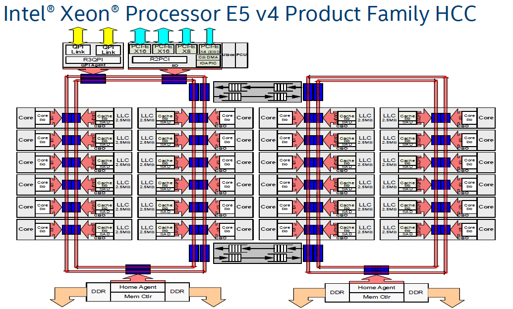
The two rings allowed for information to transfer in either direction using the two bridges to transport between the two sets of cores. This structure is incredibly important. Every time data needed to traverse to different parts of the die, it would have to hop along these rings. Each hop adds latency and there was a natural wire limitation to bandwidth. What this meant is that communication between hops on the rings could vary significantly on higher core count parts. Hops not only coincide with cores, but there are also stops on the rings for PCIe and memory controllers. For lower core count chips that were more akin to Nehalem (4C), Westmere (6C) and Sandy Bridge (8C), a single ring set can be used:
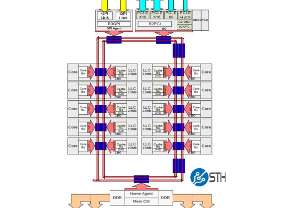
In that scenario, which powers most of the volume of Intel Xeon E5 V3 / V4 sales, the ring architecture did not need bridges and made a decent amount of sense still.
Here is an example from the Haswell generation (E7 V3) where the rings had only 18 cores to deal with but you can see the additional QPI link added for 4 socket and above connectivity:
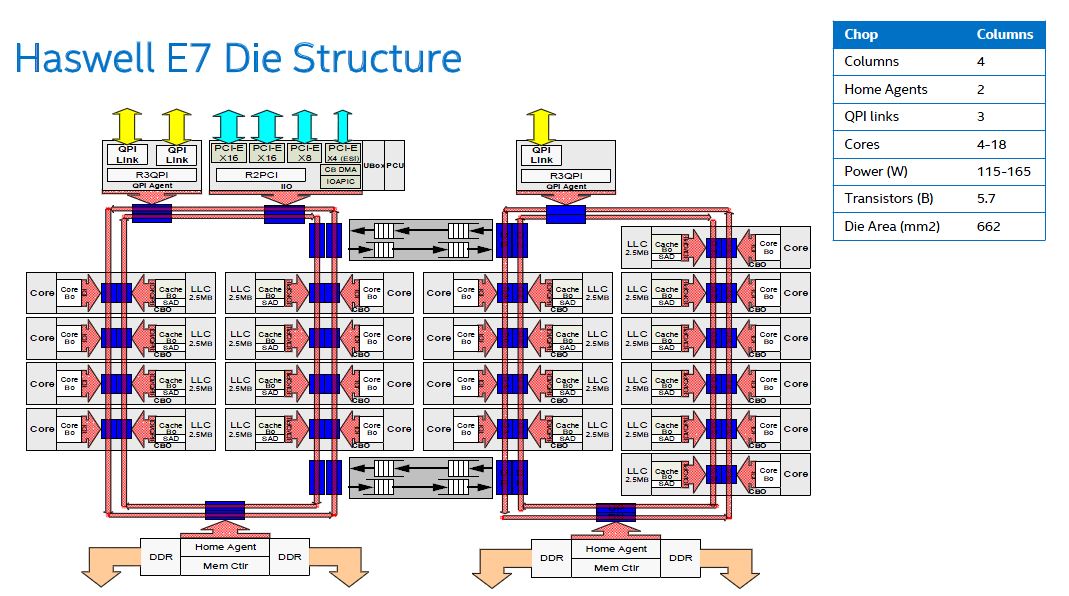
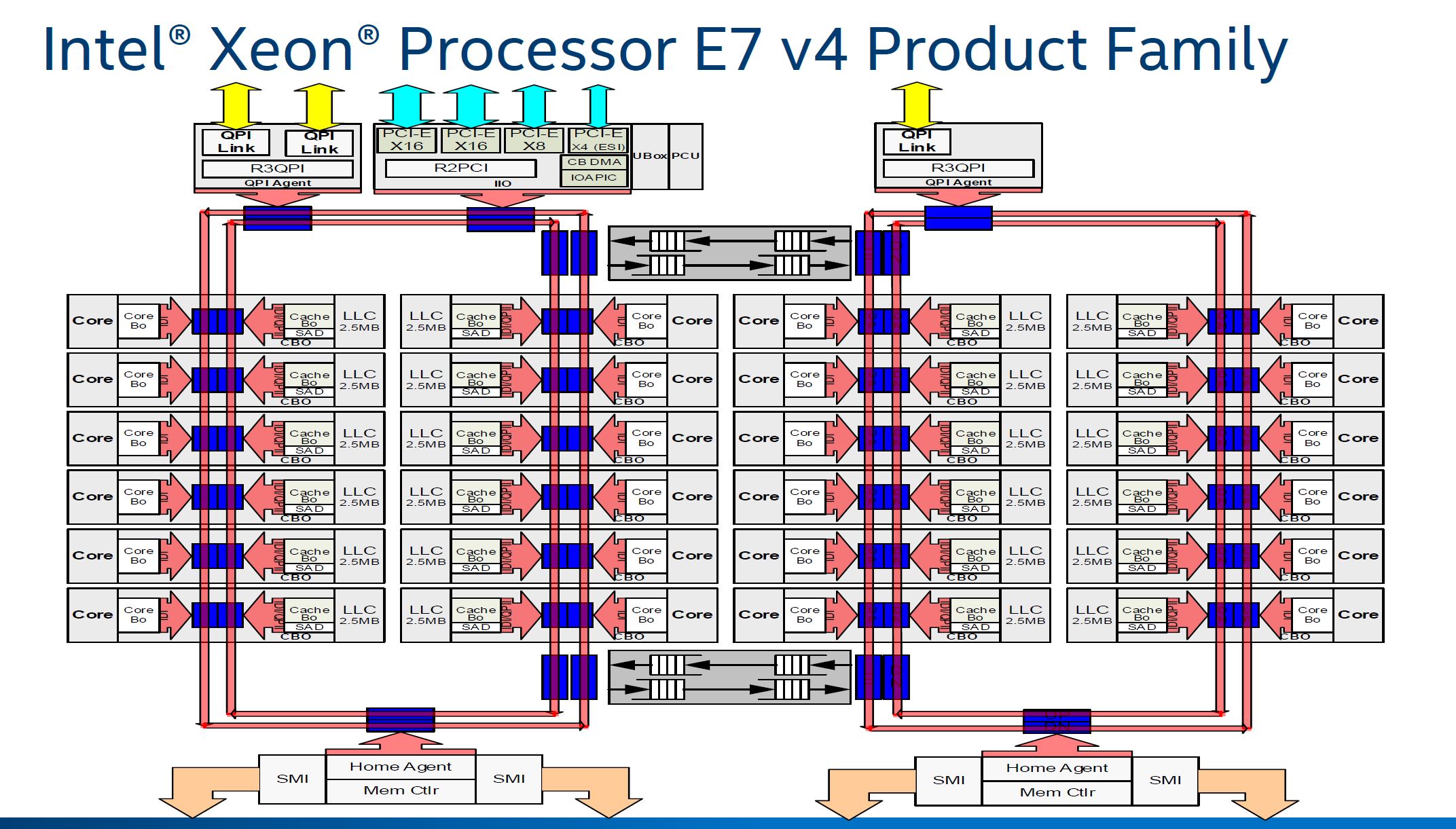
When scaled to the Intel Xeon E7 V4, you could have all 24 cores as well as the additional QPI link added. This was the configuration for our Dell PowerEdge R930 testing with the Xeon E7-8890 V4. It is easy to see how this complexity with so many cores was becoming a constraint. Remember, this architecture debuted with a 4 core part and scaled to about 6x the complexity (with some obvious modification.)
Intel needed an architecture to not only handle more cores, but eventually more I/O. The company has not been shy about FPGA, Nervana and Omni-Path integration. There are an ever increasing number of interconnection points as the chips scale to more cores and more I/O attached. For the higher core count parts, Intel needed a change. That change is mesh.
Getting Meshy with the Next-Generation Intel Skylake-SP CPUs Mesh Architecture
It turns out, there are only so many ways that these problems are solved. One of them could have been adding more bridges and more rings. Instead, with the next-generation Intel Skylake-SP, the CPUs will utilize a mesh architecture.
We received the below as an “approved” version of the mesh that we can use. We will have a more complete version that we can share during the launch coverage. While this is vague in places it does not need to be, it does help present a simple diagram for Skylake-SP and presumably future Intel architectures such as Coffee Lake.
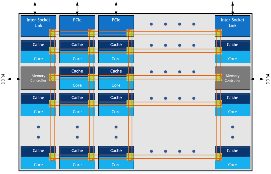
The basic premise of the above is that there are vertical and horizontal connections. Each set of connections has hops for different cores and different I/O such as PCIe and memory controllers. An astute eye may notice that Intel is using “Inter-Socket Link” not QPI in the diagram.
The key here is that instead of two sets of rings, the number of on-die communication channels Intel is opening up is exploding. This is done both to significantly increase on-die bandwidth but also to decrease latency between (most) points of the chip. Here is an example of how a memory load from DRAM may trace the structures in each architecture to a far core/ cache:
Every time one needs to traverse to a new wire or hop, there is a clock cycle penalty. Although the Skylake diagram is conceptual, it does allow you to understand how it will work in practice.
Implications of this new mesh architecture are severalfold. First, it will allow Intel to reasonably scale both cores as well as different interconnect points for PCIe or other I/O. Second, for heavy I/O applications such as NVMe SSD arrays, 100Gbps and faster networking (e.g. 100GbE, Omni-Path and Infiniband), the new architecture should provide lower maximum latency and more bandwidth.
On the PCIe side, there is an important nuance depicted. In the Skylake-SP mesh, PCIe controllers have two different mesh stops. Contrast this with Broadwell where there was only one stop for PCIe on one of the ring sets.
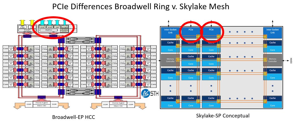
If you look at where the ring connects to the PCIe in Broadwell, you can see a potential bottleneck where there is one connection point to only one set of rings. With the new mesh architecture, there will be multiple PCIe termination points connected to the mesh. That means transfers over PCIe should be more efficient. We still expect some latency differences between cores/ cache to the mesh and PCIe but the new architecture should make a noticeable impact on latencies.
Final Words
At the end of the day, there were a number of architectural changes that needed to happen after Broadwell. The higher core count Broadwell CPUs were starting to hit the limits of memory and I/O of an aging platform. Even in smaller CPUs, we saw similar behavior. For example, the Intel Xeon D (Broadwell-DE) starts to hit limits at 16 core parts such as the Intel Xeon D-1587. Likewise, we have been able to starve AMD Ryzen 8 core / 16 thread parts for memory bandwidth with applications such as LS-Dyna. In the end, as chips become more complex, Intel needed a way to manage the complexity of having more resources connected at the heart of servers. The next generation of that management is through the new mesh architecture.


I wonder if this mesh interconnect infringes on any of Tilera’s patents?
This isn’t Intel’s first product using the mesh interconnect. They used the same general architecture in last year’s Knights Landing Xeon Phi, although I wouldn’t be surprised if there are some refinements in the Skylake Xeons.
DC – you are exactly right. KNL also used a mesh. Skylake-EP is a bit different. Also, Skylake cores are significantly different than KNL cores.
Andrew Thrift – My sense is that even if so, Intel has a fairly significant IP portfolio that can be used as defense.
Saying a mesh interconnect violates patents is like saying using dual cores violate patents. There are multiple ways to skin a cat – well in this case to make a mesh. A patent that applies it so broadly would be a bad system.
I understand there are no solid numbers concerning latencies in communication, but if I understood correctly there is 1c penalty for every hop on the mesh. How does it compare to Ring Bus in accessing L2 cache of distant core in case of a miss in L3? How does Mesh throughput compares to RingBus – if access to PCIEx happens in 2 ports it should mean that Mesh Interconnect single link is wide and fast enough to fulfill PCIEx request – are there any data on that? Does Mesh work in separate clock domain and what is it’s impact on power use of the CPU?
Great questions. Unfortunately, Intel will only let us share a very limited amount of information at this time. Stay tuned.
Found partial answer to all of them here http://www.anandtech.com/show/11550/the-intel-skylakex-review-core-i9-7900x-i7-7820x-and-i7-7800x-tested/5 – there are also tips about where to find more info – Dr Akhilesh Kumar “MoDe-X: Microarchitecture of a Layout-Aware Modular Decoupled Crossbar for On-Chip Interconnects, IEEE Transactions on Computers, Vol. 63, No. 3, March 2014 P622.”
@mat9v – Ian is very smart. I had breakfast with him and did a bus ride today in Austin.
STH will have a bit more at the Skylake-SP launch.
Oh, I know and agree, I just thirst for knowledge ;) so I went looking for more info on my own :)
But I do have a question. If I use 2P mainboard and insert only one CPU (of the 2P kind) do I have a 128 PCIEx lines to use or are they statically forced to socket communication and can not be used in another way?
Comments are closed.