
Today, Intel’s Chief Architect Raja Koduri showed off the company’s supercomputer GPU. As we saw from his SC19 keynote, this was set to be a big milestone in terms of GPU architecture. See Intel Xe HPC GPU is Something to Get Excited About. Now, that GPU is closer to reality.
Intel Xe HPC Ponte Vecchio Packaging
At Raja’s SC19 presentation, he outlined how the Ponte Vecchio GPU would be different and designed specifically for exascale supercomputing.

At the time, he said the new chip would use various technologies for connecting HBM as well as what Intel is calling the “RAMBO” cache.
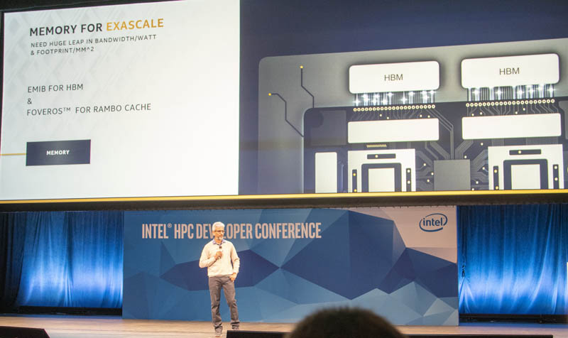
As part of that discussion, we expected a number of tiles to be integrated with different components from different fabs onto a single package.
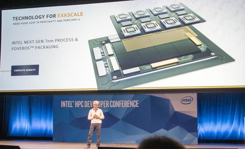
Today, we have a glimpse of what that packaging looks like and it roughly aligns with what we saw in that artist rendering around 5 quarters ago.
Xe HPC ready for power on!
7 advanced silicon technologies in a single package
Silicon engineers dream
Thing of beauty @intel pic.twitter.com/RF8Prsy05f— Raja Koduri (@Rajaontheedge) January 26, 2021
Rotating and brightening the image a bit gives us a look at the package:
From what we can see, there are 25 tiles on each side of the massive GPU. That means we are potentially looking at a GPU with what is a fairly extreme level of silicon packaging and integration effort. There also may be silicon being stacked here that we cannot see.
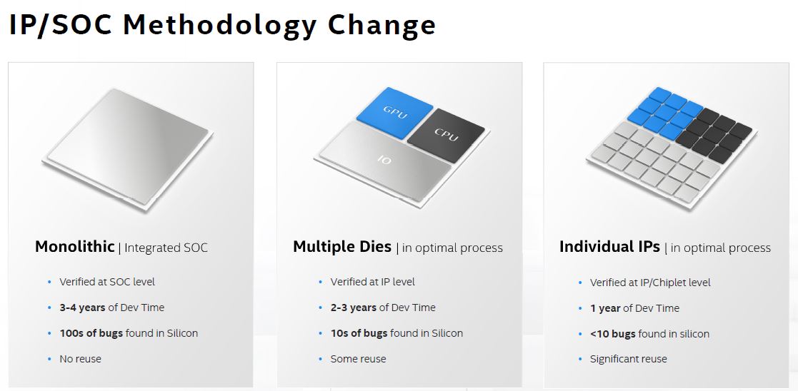
This aligns very well with the Future Intel Methodology outlined at Intel Architecture Day 2020. There, the company focused on a next-generation of packaging where it would take different IP blocks and rely on packaging to integrated into a larger system.
If we look at the Ponte Vecchio package shot today, it looks like that is exactly where Intel is heading with its new CPU.
Final Words
This is truly impressive for Intel, assuming it powers on. At the higher end of the market, we get to see some of the more exotic technologies that will eventually filter into more products. What we see in the Intel Xe HPC GPU aligns with what we are seeing Intel message as its methodology well beyond its high-end GPUs.
Intel has been touting packaging technologies as a key differentiator since it can use them to meld IP from different fabs, not just its own. This is certainly a few steps above what current-generation multi-die NVIDIA and AMD solutions offer in the GPU/ CPU space so it will be interesting to see how those players evolve to address Intel taking the next step in products.


1. That doesn’t really look like 25 dies per GPU (as tiles), more like 1 big die. + There seems to be 1 IO-
Die in the corners. You are mixing two presentations and jumping to conclusion… Did you ask Intel for PVC details?
Why would a chip of this size (compare to HBM stack) even need different dies in “optimal process”? High-End datacenter GPUs don’t need to be that cheap to have good margins. Intels 7 nm won’t be that bad or they should consider outsourcing anyway.
Chiplets/Tiles are only better than monolithic chips in two scenarios: saving money or allowing much bigger chips (without stitching).
2. “roughly aligns with what we saw in that artist rendering around 5 quarters ago”: looks significantly different.
3. You are comparing it to “current-generation multi-die NVIDIA and AMD solutions”
but when is this supposed to come to market with Intel 7 nm products arriving (maybe) in 2023?
@lasertoe The big block in the middle is made of >10 dies 3d stacked (foveros) on top of a large base die. Each small block is separate piece of silicon. It’s not a single big die..
The main “compute tiles” are NOT made up of “20 separate dies”. Aka, there are NOT “25 tiles per side”!
Rather, despite the way it may initially seem, there’s actually just 6x dies per side (1x large compute tile, 2x HBM2e stacks, 2x Rambo Cache tiles, & 1x I/O tile), or 12 distinct, physical chips in total.
This is because the main compute tiles in the center are actually single, monolithic dies that are made up of a bunch of distinct sections which are actually fabbed with COMPLETELY different manufacturing nodes (specifically 7nm Intel & “next-gen TSMC” [prolly 3nm]).
This is why it appears “divided into smaller chips”, even when it’s actually physically all one die. It’s to separate the parts using different fabrication nodes. Some are Intel 7nm fabbed, others are TSMC 3nm fabbed, & it’s likely a few of these “sections” are simply there for fabrication redundancy.
What this means is that the uncut, compute tile wafers are actually sent from one fab (say Intel’s 7nm one) to the other (TSMC 3nm) after they’ve printed only “their” sections of the chip. But just because it’s fabbed in distinct, smaller sections, using 2x different nodes, does NOT mean they are all actually fully separate/cut apart silicon dies.
Given those tiles are on the same substrate I doubt Intel is going to see double digits yield numbers. Even within a single production line miniscule offsets between steps can destroy an entire die and now Intel wants us to believe it can transfer dies between fabs and have working silicon at the end? Why they’re not going with chiplets is a true mystery to me.
@Cooe I initially thought you had a point, until you mentioned that they were printing different nodes on the same die. I cannot fathom how you came up with this explanation, but from my limited knowledge of EE, I do not think that alignment technologies have their accuracies increased to a point where you can ship a die from Taiwan to the US and still keep the same alignment, not to mention the nightmare to have intel and TSMC — both using different materials for their gates — to have the doping not interfere with each other. Thus, I would say that this, which no fab, not TSMC, not Samsung, and not Intel, could do, is probably not tried at this monstrous scale(HPC) off the bat.
@Lasertoe I initially thought so too, until I saw a comment somewhere a person explaining the different tiles, I will paste that comment below :
“I believe this is a Co-EMIB design with two reticle-limit sized Foveros stacks. Each Foveros module contains 8 XeCU dies (the more or less square ones). The RAMBO caches are the 8 smaller dies in-between the 16 XeCU dies. The 12 dies flanking the XeCU dies on the outside of the modules are the XeMF dies. The four small dies where the two modules abut are probably for the on-package CXL links or whatever I/O they’re using between modules. Then there are 8 HBM2E stacks and two transceiver tiles sharing the organic substrate which are connected to the Foveros stacks via EMIB. It seems like the lower die in the Foveros stack may be more like a traditional silicon interposer.”
So turns out we might BOTH be right, lol. The part about the compute tiles being fabbed at BOTH Intel 7nm & TSMC “next-gen” (either 5nm or 3nm) comes straight from Intel’s mouth.
That means they’re either ->
1. Fabbed partly on both as I originally suggested (which would DEFINITELY be a “next-gen” chip packaging tech worth bragging about & would explain the subdivisions).
2. TSMC’s just being used as an old-school second source, 1970’s/80’s style (really unlikely IMO).
3. Or finally that those 20x subdivisions on the complete compute tile ARE actually separate chiplets (with the 2 different sizes being the 2 different fab nodes) but they are mounted to a large, monolithic interposer underneath (which could be what Intel is calling the “Base tile”).
But regardless, the chip actually mounted onto the MCM package itself IS monolithic, be that the compute die itself or a huge interposer underneath 20x separate chiplets. And both TSMC & Intel are being used to fab the “compute tile” (which Intel always refers to singularly, making this all the more confusing if it IS actually multiple chiplets on an interposer….)
https://www.anandtech.com/show/15188/analyzing-intels-discrete-xe-hpc-graphics-disclosure-ponte-vecchio/3
@yp
The reason why I’m saying this is one die is because the reflections are uniform on the chips in the middle but vary on the outside chips. This might be a photoshopped pic.
Some addition:
1. There is no such thing as a standard “reticle size” when it comes to advanced packaging because you are not limited to 4x shrink of a mask to 32x26mm^2. You (and the “journalists who keep repeating that) should get that out of your system.
KrF example with 33×42 reticles: https://global.canon/en/product/indtech/semicon/fpa6300esw.html
i-line example with 50×50 exposure: https://global.canon/en/product/indtech/semicon/fpa5510ix.html
That’s also how TSMC is doing their 2x reticle size CoWoS.
You can even do no shrink on ArF if you want. With Intel buying customized Litho from Nikon that should be no problem at all and the costs are next to nothing compared to their CapEx.
2. These chips are nowhere near “reticle size” limits. Compare the big chips relative size to HBM stacks with Nvidia GA100 to HBM2.
3. i still didn’t hear one good reason why this shouldn’t be just one die at this size. Redundancy is also built into other GPU like GA100 where a lot of CUs and even on memory controller/PHY are deactivated.
It gets even weirder when we see that many of those tiles won’t be reused on other/client Xe GPUs because they are clearly HPC “tiles”.
Something is clearly not right here:
At ~650mm2 (looks even smaller than that) you get about 100 chips per wafer. With a TSMC 5nm defect rate of typically 100×0.9^6.5 ~=50 perfect chips.
Even if Intel is building on a crappy node with 35% defects per 100mm2 that sould still make about 6 good dies per wafer and that should be enough to build Aurora with reasonable margins.
4. This partitioning to these extreme levels makes no sense because while they would help the yield a little, the power consumption for additional chip to chip communication would rise (even with better C2C PHYs).
HPC GPUs are especially sensitive to power because all kinds of units are transferring data all the time and the clock is clearly limited by power.
Having 30mm^2 big dies/tiles seems ridiculous as 100-200mm2 big tiles should have good enough yields even on a bad/unfinished node (like 0.5 per 100mm2).
Something is wrong with the HBM stacks:
In Rajas pic the left stacks are 20% smaller than the right stacks.
This is probably just an artist’s depiction of PVC.
Forget about everything I said.
Waste of time.Intel marketing .
This is a monster but the Intel packaging team is the best on the planet and they might get a couple to work. In the long run, I don’t believe this will scale and it will become a test and manufacturing nightmare with terrible yields.
Simplicity wins, always.
Comments are closed.