
What would we call disaggregation of a SoC (System-on-Chip) disaggregation to something more akin to a SoP (System-on-Package) approach? We are going to use SoC Containerization to communicate the concept here. As part of Intel Architecture Day 2020, Intel showed a number of technical advancements. There was a very short portion of the presentation dedicated to its future SoC and IP methodology which has some stark potential to change the way Intel presents itself in the market.
“SoC Containerization” Future Methodology
Packaging sounds abstract, but if you look at what Intel is doing today, there are a few dies being integrated. Intel is looking well beyond doing a handful of dies such as with Lakefield. Instead, the company is moving from monolithic dies to multiple dies and eventually to individual IP blocks.
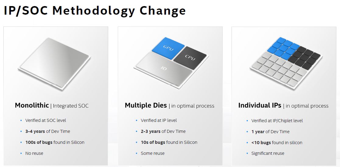
Of particular note, Intel here has the GPU, CPU, and IO die separately illustrated. That looks a lot more like an AMD model of disaggregation. It also makes a lot of sense since we would likely have either PCIe Gen4 or Ice Lake Xeon cores today if Intel had moved to I/O die and disaggregation in this generation. The individual IPs are where this gets fascinating. Here is an illustration:
This has huge applications beyond the client space. For example, what if Intel on the Xeon side had four versions of the Xeon Gold 6520 (fictional part)? There could be a:
- Xeon Gold 6520A – ASPEED BMC
- Xeon Gold 6520D – Dell iDRAC BMC
- Xeon Gold 6520H – HPE iLO BMC
- Xeon Gold 6520L – Lenovo XClarity Controller BMC
- Xeon Gold 6520G – Google Custom BMC
That would mean that the Xeon you buy from Dell would be different than Supermicro or HPE. Incidentally, integrating an ASPEED BMC would have a fairly significant server motherboard area reclamation impact especially if DRAM and NAND chips could be stacked and integrated.
One way to productize this is that Intel could define the IP blocks. For example, Intel could have a media codec block that was different for a future Core i9 than a future Core i3 and that could be the same across different IP blocks.
The other way this could be productized is to allow OEMs and customers to define chiplets used and therefore products. Dell could have a Intel Core iDell-1370 that uses different IP blocks than an Intel Core iHP-1370.
Could one put a Core iHP into a Dell system and should that work? If not, then we are going down a path of limited hardware recyclability which is not an eco-friendly approach. If it does work, then does Quanta make the notebook and HP or Dell’s value-add become less about the mechanical design and more about the SoC design and distribution chain? What if the Dell server part has a specific VMware optimization and vSphere license tied to the actual chip IP block? There is a ton to unpack with this model.
Final Words
I asked Raja about this strategy, and he referred me to the presentation since he did not want to make a new disclosure.
What I will say is that if this is truly Intel’s direction, then defining this strategy and building the chiplet ecosystem could be, by far, the most important job at the company. If you look at PC’s from pre-2000 they were cobbled together with IP blocks represented by ISA, PCI, accelerator socket, and even modular cache slots. Over time, the GPU moved to the SoC. The audio went from being an add-in card to being a small motherboard chip. The same happened to network connectivity. In the future, audio and networking could move to a chiplet making for a true SoC (or SoP.) Today’s motherboards effectively become tomorrow’s SoPs.
True disaggregation to chiplet IP blocks is what we are going to call “SoC Containerization.” Instead of a monolithic software application or hardware SoC, one gets a solution built of lower-level components. These lower-level components can be iterated on at different rates, much like a container-based software application.


“That would mean that the Xeon you buy from Dell would be different than Supermicro or HPE. Incidentally, integrating an ASPEED BMC would have a fairly significant server motherboard area reclamation impact especially if DRAM and NAND chips could be stacked and integrated.”
I would imagine and have seen OEMs and business recoil from having such vendor specific CPUs, that would mean Intel/OEM must keep sufficient stock of all particular SKUs for warranty purposes which is much harder when you have such a broken down product stack. You want to homogenise your products so that you dip and nab as you need not have to produce a bunch of wasted space until its needed.
Your point is understood, but very wasteful.
Emile – Dell is already doing this in a way in some product lines. E.g. You cannot take a Dell chip and put it in a Supermicro or HPE server. We are going to cover this soon.
Interesting.
Does this mean there are going to be “blank” areas in the chips which need microcode stored in the UEFI to be loaded? Is this somehow related to FPGAs being included on future Xeons?
Imagine the product stack if this goes ahead. Instead of being a 2D table, we will have to deal with a hypercube with at least 4 dimensions. The idea is neat, but Intel will split every hair into at least 4 new SKUs.
SiP = System In Package. Defined long ago. No need for ‘SoP’…. ;-)
Its a beneficial approach – but its not free, and there is an optimum level of ‘dicing’ that has to be found on a case-by-case basis. Too many die, and the cost (and overall size – due to the space between) goes up. Too few, and yields and flexibility (and cost) take a hit.
Right now, AMD has got it just right it seems.
For a company already struggling with supply and an ever-increasing SKU complexity, making multiple custom products for every vendor sounds like a noose to me…. it won’t bring anymore money to Intel, HP (for instance) won’t pay more for their ‘secret flavor’, it’ll just turn into a massive headache trying to manage the supply channel…. I don’t see them doing that honestly.
I’m failing to see how this can be a good idea. It seems that this is a potential step backward AWAY from universally standardized CPUs and other components and toward a model of “custom” parts that are mutually incompatible and won’t work with any motherboard except that of the company whose “custom” processor you bought. And the cost of all this to the end user will hurt BADLY.
This may not be an issue for server and mainframe systems which already cost hundreds of thousands to tens of millions of dollars, but it would be very detrimental to the far more price-sensitive single-user workstation and home computer market. Not only would this stand to increase the price of systems and components to the end users buying them, this could result in higher manufacturing costs as the companies making these brand-specific custom processors would be forced to maintain full stock of multiple different versions of the same model number and SKU parts.
It’s one thing to integrate the GPU and some I/O into a processor as a means of simplifying the process of building a machine from scratch so that less well-heeled buyers can have graphics capability while not being forced to take out a second mortgage just to have the funds for a discrete graphics card, many of which cost almost as much as another whole computer. But it’s quite another to make a custom-configured processor that’s brand-locked and won’t work in a motherboard that has slightly differing features from what the CPU chip expects to see, meaning that if the original board dies or you decide to upgrade without buying a new CPU, hoping you can still use it, you might well be screwed and hard. And there’d be absolutely NO guarantee that the OEM would even let you buy the appropriate CPU anyway. I sadly can only see this as another case of Apple syndrome, except it won’t hurt just Mac users. No, no, it will hurt absolutely EVERYBODY.
Personally, I don’t want to buy, nor do I relish buying, a computer that’s using a CPU or other mostly standard normally readily replaceable or transferrable component that’s been designed in a manner that if I had to upgrade or replace that component for any reason it won’t work in the new configuration. Please let me be wrong and let’s hope this new “methodology” of Intel’s will prove no worse an experience than what’s already been suffered by the computer industry thus far.
I think people are overly focused on the integrated BMC angle, which seems like mostly (entirely?) conjecture.
Another narrative could be, this is the logical next step for having configurable graphics options. Look at Crystal Well, which added a large eDRAM die for graphics performance, followed by Kaby Lake-G which is another attempt at better single-package graphics. Now that Intel has serious ambitions for their own graphics ip and they happen to have all this fancy packaging tech, this was sort of inevitable.
I remember people were speculating that the original client Zen 2 IO die would be reused for APUs with one cpu and one gpu chiplet, which is basically the same vision.
@Jim – yes, there’s nothing new about this. its been going on for years. Its a bit amusing that Intel can come up and say ‘we’re going to do this, but…. wait for it…. our die will be smaller and the configurations more flexible’ and expect a round of applause at the revolutionary approach!
It makes sense to co-package die with different process requirements – analog, digital, power, memory… all often have different requirements and one-die, one-process with the capability for all is often an expensive way to go. All the IC companies have been doing that routinely for over a decade for much smaller designs than processors. i think most people probably be surprised how many (even as small as 20-pin) IC’s are infact multi-die co-package solutions, you can’t tell from the outside. Any package type can hide multiple die on the inside, but most people don’t know or care.
I am not sure about it.
At some point, and my guess is soon enough Transfer energy per bit it going to eat into the equation. i.e the Optimal Power Efficiency will always be Monolithic.
While I agree with some of the point, I cant help but think most of these advantage are very Intel specific, and dont translate into other products especially those that are already licensing IP and Fabs at TSMC. But I know the Internet will take it Intel is still in the lead with Alien Tech and Containerisation is the “only” way to go .
Comments are closed.