
At Intel Architecture Day 2020, the company highlighted its new process and packaging techniques in a big way. In this article, we are going to discuss some of the changes Intel is making including new disclosures around its 10nm node and a look at its packaging technology roadmap.
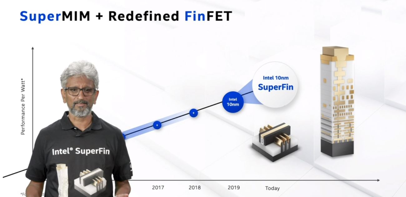
Intel 10nm FinFET SuperFin and Enhanced SuperFin
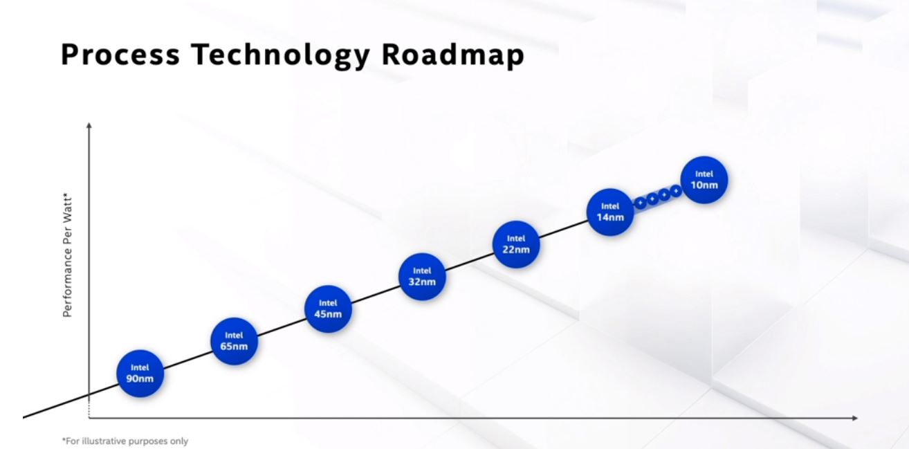
Perhaps one of the slide that will make many in the industry smile (or smirk) is the technology roadmap slide for Intel’s process technology. It is being displayed with a near linear progression with fairly even spacing between nodes on an unlabeled X-axis. The “performance per watt” Y-axis is for illustrative purposes only which we read as “what we hoped would happen.” Still, the point being made is that Intel pushed 14nm and got gains before transitioning to 10nm.
Intel discussed some of its 10nm FinFET advancements. These advancements also coincided with a severely delayed 10nm process which was not part of this presentation, although Intel did acknowledge that 10nm is behind initial projected delivery timelines.
As part of its 10nm program, Intel is re-designing some key parts. For example, Intel has new FinFET advancements in this generation. Effectively, Intel’s disclosures are leading up to the notion that we are not just getting the initial 10nm version, but there are improvements going into the node already.
Intel is calling this update to its 10nm FinFET the “10nm SuperFin.” For those accustomed to the 14nm nomenclature, this is analogous to a 10nm+. With SuperFin, via the Intel Fact Sheet:
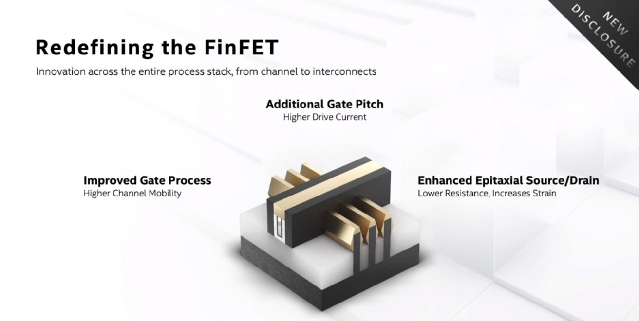
- Enhancing epitaxial growth of crystal structures on the source and drain, thus increasing strain and reducing resistance to allow more current through the channel.
- Improving the gate process to drive higher channel mobility, which enables charge carriers to move more quickly.
- Providing an additional gate pitch option for higher drive current in certain chip functions that require the utmost performance.
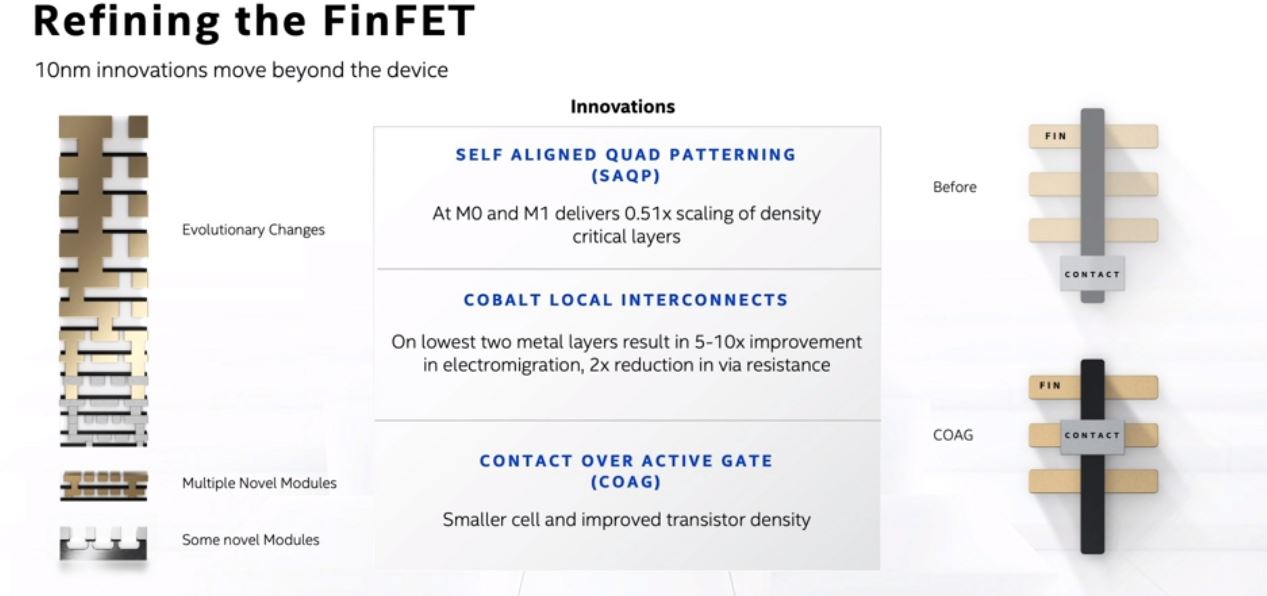
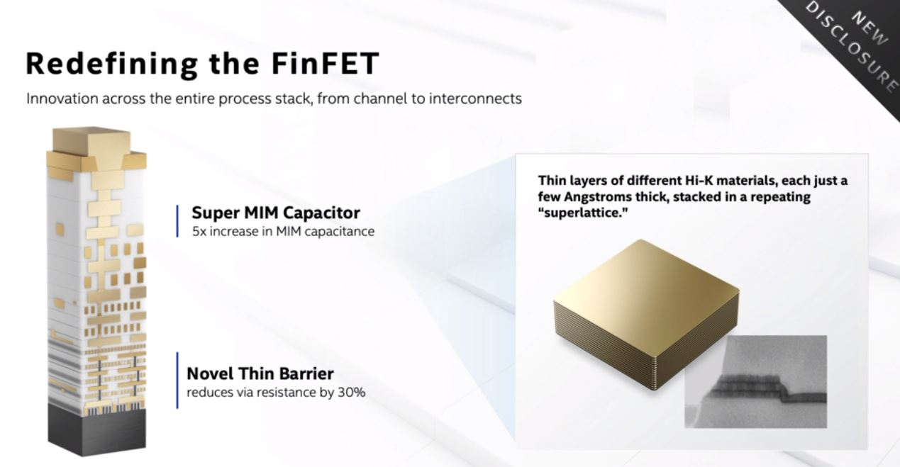
- Using a novel thin barrier to reduce resistance by 30% and enhance interconnect performance.
- Delivering a 5x increase in capacitance within the same footprint when compared to industry standard, driving a voltage droop reduction that translates to dramatically improved product performance. The technology is enabled by a new class of “Hi-K” dielectric materials stacked in ultra-thin layers just several angstroms thick to form a repeating “super lattice” structure. (Source: Intel)
We were told that the upcoming (soon) Tiger Lake consumer parts will utilize this 10nm SuperFin process.
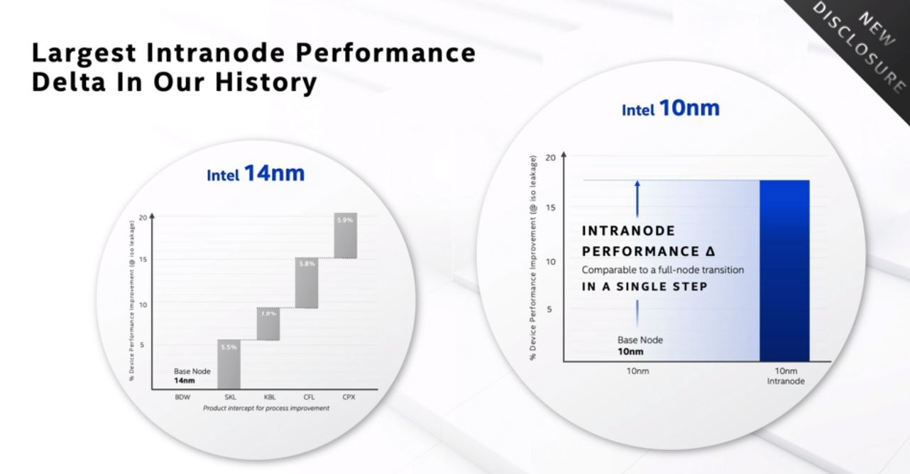
The net impact is that Intel is seeing a 15-20% intranode performance jump with 10nm SuperFin that it equates to benefits from a full node transition. In layman’s terms, Intel says the new 10nm SuperFin is much better than its initial 10nm products.
There is a version of this slide without Raja in the “Intel SuperFin” shirt, but it seemed imprudent not to include this detail.
Going beyond 10nm SuperFin (or 10nm+) we have 10nm Enhanced SuperFin (10nm++?) that helps drive higher bandwidth interconnects for the data center products.
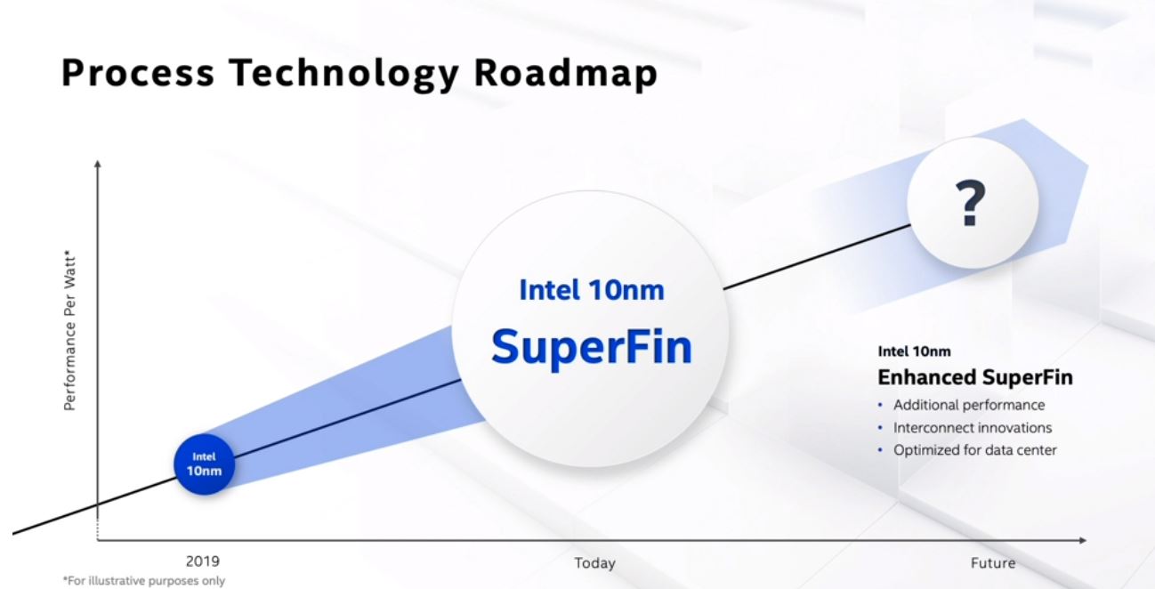
We are going to cover data center products in another article on Ice Lake Xeon (and Xeon D) along with Sapphire Rapids. It seems interesting that after very few products launched on the original 10nm process, we are getting an update (or two) with major product lines finally transitioning. In some ways, 10nm SuperFin feels more like it is what will be remembered as the 10nm launch while the original 10nm process will be the technical launch.
Next, we are going to get to the packaging technology.
Intel Packaging Technology Architecture Day 2020
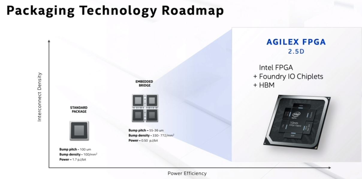
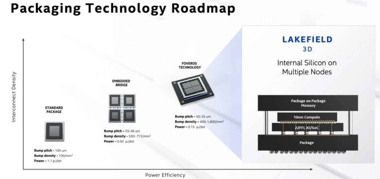
Intel had a build slide for its packaging technology roadmap, but we decided to simply showcase the fully-built version and discuss where we are going beyond a standard monolithic die package.
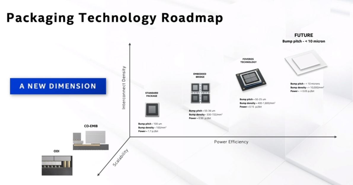
New EMIB 2.5D packaging started with Kaby Lake G but is perhaps being used most effectively with Agilex.
One of the big features that Intel is trying to push is this idea of package-level integration. Effectively it can put different IP blocks on different chiplets and manufacturing nodes. This can be Intel designed and/or fabbed chiplets as well as third party chiplets and put them together.
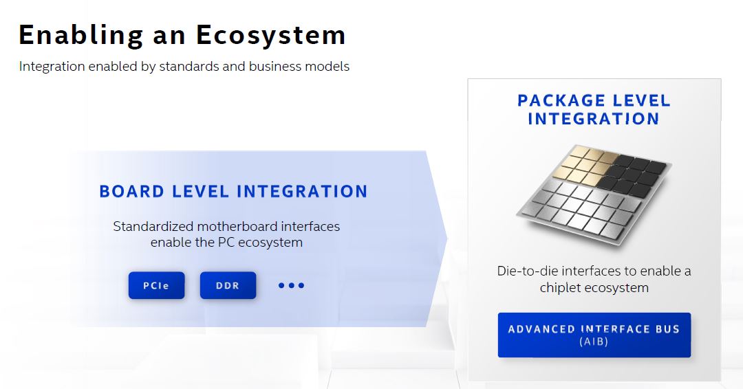
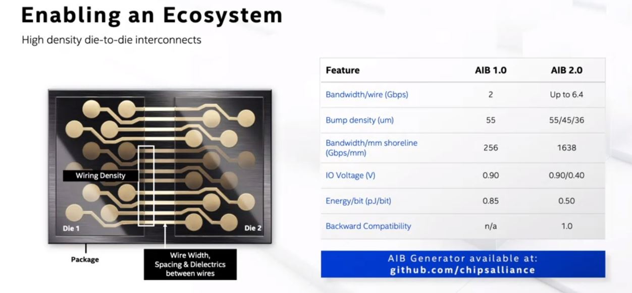
Part of this technology is the Intel Advanced Interface Bus or AIB. AIB 2.0 brings massive jumps in terms of bandwidth and density. It also brings power savings. In effect, Intel is trying to jumpstart a larger ecosystem where it is a chip integrator, not just a designer and manufacturer. This is a big deal. Implicit in this posture is that Intel is recognizing it cannot design the best everything in silicon.
We covered Intel Foveros is Awesome Do Not Worry before, but it is Intel’s 3D die stacking technology.
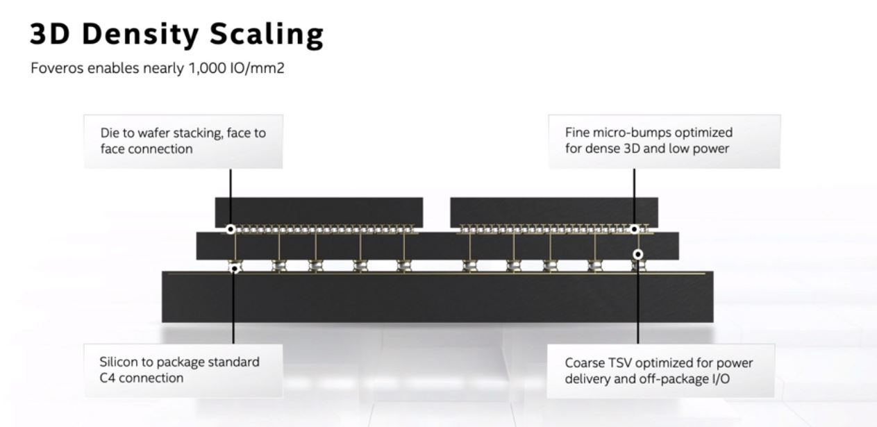
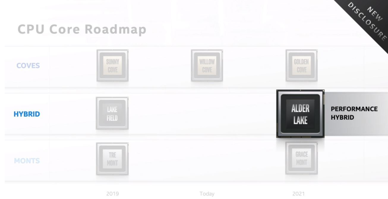
Lakefield was the first product to use 3D die stacking. We see this more as a proof point of the technology at this point rather than something that Intel is putting in its mainstream parts immediately.
Indeed, Intel discussed how Alder Lake would be a 2021 higher-performance hybrid. From the Architecture Day discussion, it seemed like Lakefield was the commercial proof of concept and Alder Lake will be the next-gen looking to go after more performance-sensitive markets. Also on the roadmap, we will notice there is a new Atom Gracemont architecture but nothing slated for 2020.
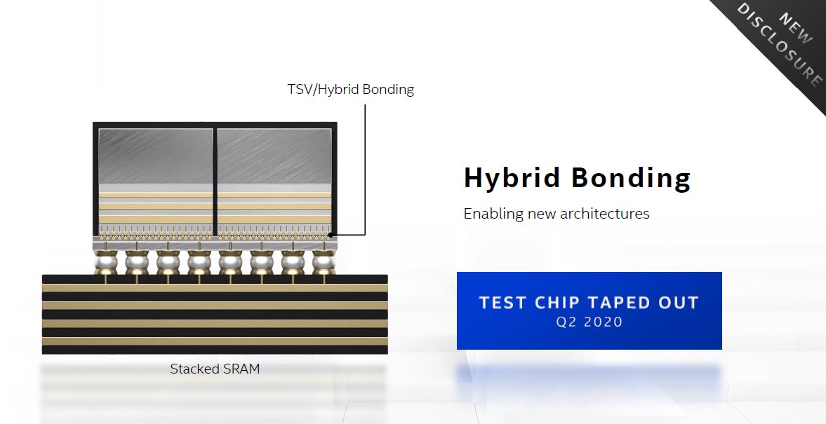
The future of technology will go beyond Foveros. Intel is looking at hybrid bonding to greatly increase the bump counts. Bumps, for those who do not know, one can think of them as wire ends exposed at the end of a chip. More bumps mean more chip-to-chip wire connections. More connections can mean more bandwidth.
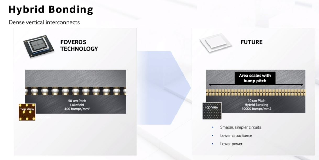
Intel says it already has done a tape-out of the new chips using this bonding technique but it is still some time away from productization.
Intel also discussed Co-EMIB. Here we have EMIB plus stacking. Using this approach, Intel can integrate IP and chiplets potentially from third parties, and build larger more complex chip structures.
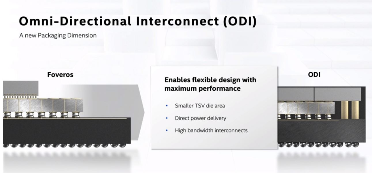
ODI is interesting because we get packaging where the top chips can overhang lower-levels of chips and get rid of some of the TSV areas used through the different layers of silicon. TSVs use die area, so ODI helps alleviate that.
If nothing else, it is clear that Intel is firmly thinking about packaging.
Final Words
The packaging technology itself is unique, but there seems to be more going on here at Intel than simply stacking a few pieces of silicon together. We are going to talk about Intel’s vision of SoC (System-on-Chip) disaggregation to something more akin to a SoP (System-on-Package) approach. We are going to call that SoC Containerization and discuss this in a separate piece.
What we do know is that as we move into the PCIe Gen5 era, Intel’s products will increasingly rely upon aggregating pieces of silicon whether they are from the company’s own designs and wafers, or from others. Traditionally we have thought of Intel as a vertically integrated design and manufacturing company. In the future, there may be a larger integration business.

