

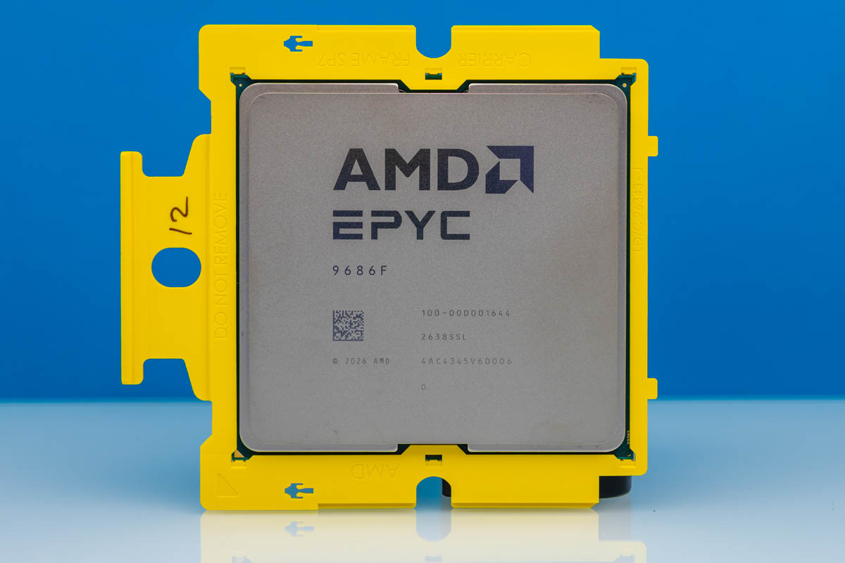
At long last, the day is here. Today, we finally get to share with you our first look at AMD’s EPYC “Venice” series, or the EPYC 9006 processors. Following AMD’s biennial CPU development roadmap, the highlight of the year for AMD’s CPU teams is the launch of the EPYC 9006 processors and the Zen 6 CPU architecture that underlies them. Amid an unprecedented explosion in demand for server CPUs for AI systems driving both host nodes and agentic workloads, AMD is in a commanding position, bringing to market a new generation of even more powerful server hardware right when the industry needs it most. All the while, AMD has ambitions of becoming the undisputed market leader for server CPUs, ambitions that Venice seems primed to help AMD reach.
As far as server CPU launches go, today’s launch is remarkable on multiple levels. Besides taking a look at a wholly new server platform from AMD (socket and all), which would normally be a big event in and of itself, the server boom has turned the CPU development cycle on its head, and now it is a server CPU where we will see AMD’s latest CPU architecture. So along with our first benchmarks of Venice, today also marks our first chance to evaluate the Zen 6 CPU architecture that will be driving so many AMD products over the coming two years – everything ranging from server chips like Venice and Verano to consumer desktops, laptops, and more. There is a lot to unpack with today’s launch.
| AMD EPYC: Generation on Generation | |||
| EPYC 9004 | EPYC 9005 | EPYC 9006 (SP7) | |
| Codename | Genoa | Turin | Venice |
| Microarchitecture | Zen 4 | Zen 5c | Zen 6c |
| Core Manufacturing | 5nm | 3nm | 2nm |
| Max Cores/Threads | 128/256 | 192/384 | 256/512 |
| Core Complex | 16 + 32MB | 16 + 32MB | 32 + 128MB |
| Memory Support | 12x DDR5-4800 | 12x DDR5-6400 | 16x DDR5-8000 / MRDIMM-12800 |
| Memory Capacity | 6TB | 6TB | 8TB |
| PCIe (1P) | 5.0 x128 | 5.0 x128 | 6.0 x96 |
| Socket | SP5 | SP5 | SP7 |
| Peak Power | 400W | 500W | 600W |
With so much to do and so little time to do it all, we are going to have a lot more content to follow. But to get things started, for today’s launch piece we are going to run the flagship EPYC 9996 through not only our agentic-workload-focused AgentSTH V7 benchmark suite, but we are also including bits and pieces of what is essentially a preview of 2027’s AgentSTH V8. For some context, we are going back roughly a decade in server architectures to not just blindly pick up benchmark suites, but to profile workloads on dozens of platforms for inclusion in the suite.
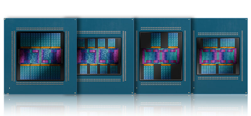
We have lots of numbers for this one and some neat comparison points. The headline feature is that we now get up to 256 cores per socket, a new PCIe Gen6 I/O subsystem, and more than twice the memory bandwidth to go along with a revised Zen 6 microarchitecture and SoC design. AMD is also splitting its lineup into multiple families for different applications with two primary sockets, a return of the -X high-cache parts with Venice-X, and the LPDDR5X Verano. The new series covers a lot more and is by far the most ambitious innovation in the EPYC line since the switch to an I/O die, which allowed the EPYC 7002 to deliver a knockout. This is the Knockout Part Deux.
I also wanted to recognize Ryan, Sam, and Vic for helping us turn this around quickly. We will have Ryan cover the Zen 6/6c microarchitecture and SoC portion before I take back over on performance. Regular STH readers may have noticed this, but many of our pieces are much longer than they used to be, and doing these reviews has become a team effort.
AMD EPYC 9006 “Venice”: The Story So Far
Over the summer, AMD held a proper unveiling for its EPYC 9006 “Venice” server CPU platform at the company’s annual Advancing AI event. In what has become AMD’s marquee event of the year – and a reflection of the importance of server parts to their bottom line – the company laid out an aggressive plan for 2026 and beyond. Spearheaded by the Venice CPU platform, AMD has ambitions to deliver not only its most powerful and most capable server platform to date, but to iterate on that over the next year or so to deliver a broad portfolio of server chips that covers everything from rank-and-file servers to mighty HPC systems, and of course lots of AI nodes.
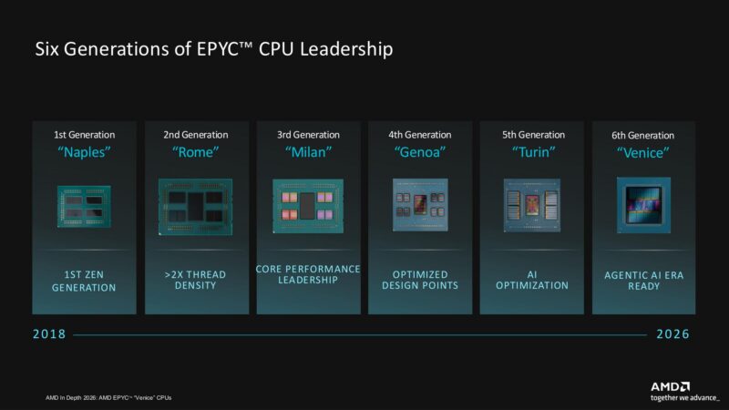
Now in its sixth generation of Zen-architecture server chips, Venice is in some respects AMD’s most aggressive design yet. AMD is making heavier use of chiplets than ever before, and the company is now relying on advanced packaging techniques to tie them all together. This has allowed AMD to fully leverage TSMC’s N2 (2nm) process node, their first GAAFET-based node, to the best of their abilities, tapping it to not only devote more transistors than ever to the Zen CPU cores to boost their performance, but to pack in more CPU cores than ever before.
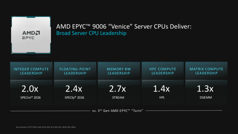
For high-throughput workloads, the highlight of Venice is that there are now up to 256 CPU cores in a single socket, a 33% improvement over EPYC 9005 “Turin” only a generation ago, and with 20% higher IPC and higher clock speeds on top of that. Meanwhile, for workloads where single-threaded performance and latency are more critical, AMD is bringing the 5.3GHz EPYC 9686F to market to double down on Zen 6’s IPC improvements with the highest clock speeds yet for an EPYC server chip.
AMD is keen to tap into the agentic era of computing. And there are a lot of improvements to Venice and the Zen 6 CPU architecture that are going to help them get there. But do not underestimate the chip in other areas, either. AMD has invested in features such as PCIe Gen6, new virtualization and security features, and it has even picked up a software engineering firm in recent months to develop software to replace DRAM with flash memory. AI is certainly the highlight of the Venice story, but it is not the only story.
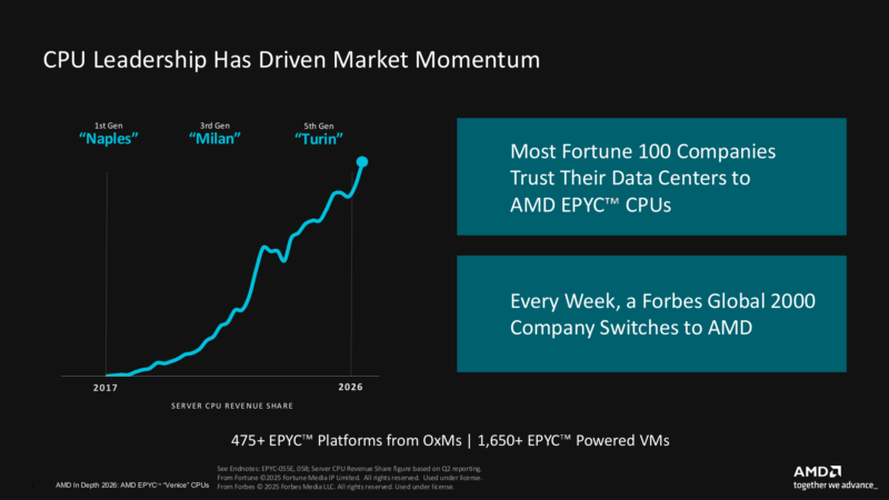
With any luck, AMD expects that over the next 12 months they will finally reach the point where they capture leadership of the server CPU market. As we saw with AMD’s earnings last week, the company’s data center division is already projecting that its revenues will surpass Intel’s in Q4 of this year. Meanwhile, AMD already holds 46% of the x86 server CPU revenue share, and the company seems confident that Venice will push it above 50% for the first time.
EPYC 9006 SP7 Product Stack: Venice Gets a Spec Bump
Alongside its initial summer announcement of the EPYC 9006 lineup, AMD also published the complete specifications for its full stack of Venice chip SKUs. This was for both the high-end SP7 platform launching today, as well as the more restrained SP8 platform that is launching early next year.
As it turns out, AMD was sandbagging things a bit. Whereas their flagship high-frequency chip, the EPYC 9686F, was originally announced to ship with a peak frequency of 5.0GHz, that is no longer the case.
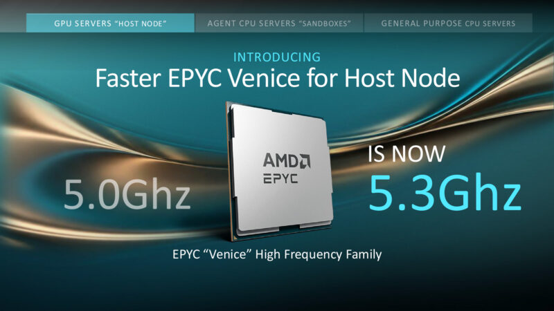
Instead, the 9686F is now a 5.3GHz chip. Making this a notable improvement just ahead of the launch of the hardware, and admittedly a bit of a point of pride (or at least bragging rights) for AMD.
In talking with AMD, the company tells us that they have found that the final silicon for their Zen 6 and Zen 6c CCDs has turned out even better than the company was expecting. Consequently, their earlier SKU stack was a bit conservative with clockspeeds, and they can do a bit better than 5.0GHz – ultimately allowing the fastest Venice to clock higher than the fastest Turin after all.
In fact, almost the entire SP7 lineup has received a clockspeed bump. Outside of the flagship EPYC 9996, every other chip in the stack has seen its max boost clockspeeds revised upwards. Now there is not a single chip with a peak clockspeed lower than 4.1GHz (Zen 6c parts), while all of the high-frequency Zen 6 parts now top out at 5.3GHz. Base clockspeeds have been revised upwards as well, with most chips picking up around 100MHz compared to AMD’s preliminary specifications.
So here is what the final, shipping SP7 chip stack looks like.
| AMD EPYC 9006 SP7 SKUs | ||||||
| CPU Cores | Threads | Max Boost Clock | Base Clock | L3 Cache | TDP | |
| AMD EPYC 9996 | 256 | 512 | 4.1 GHz | 2.55 GHz | 1024 MB | 600W |
| AMD EPYC 9966 | 192 | 384 | 4.1 GHz | 3.05 GHz | 768 MB | 600W |
| AMD EPYC 9956 | 256 | 512 | 4.1 GHz | 1.7 GHz | 1024 MB | 400W |
| AMD EPYC 9846 | 168 | 336 | 4.1 GHz | 2.9 GHz | 768 MB | 500W |
| AMD EPYC 9756 | 128 | 256 | 4.1 GHz | 3.2 GHz | 512 MB | 500W |
| AMD EPYC 9G76 | 96 | 192 | 5.3 GHz | 3.65 GHz | 384 MB | 500W |
| AMD EPYC 9686F | 96 | 192 | 5.3 GHz | 4.05 GHz | 384 MB | 600W |
| AMD EPYC 9656 | 96 | 192 | 4.1 GHz | 2.85 GHz | 512 MB | 400W |
| AMD EPYC 9586F | 64 | 128 | 5.3 GHz | 4.05 GHz | 384 MB | 400W |
| AMD EPYC 9556 | 64 | 128 | 5.1 GHz | 3.6 GHz | 192 MB | 400W |
AMD has also used this opportunity to sneak in one last chip SKU ahead of today’s launch. The EPYC 9956 has been added to the product stack; this is a lower clocked version of AMD’s biggest 256 core configuration, with a similarly reduced TDP of 400 Watts. So AMD’s customers now have a couple of options if they want a high throughput 256 core part.


Excellent review, very impressive detail level and benchmarks. SKU table on first page needs an update vs AMD website documentation.
Thank you for the kind words. The SKU table has been updated; AMD hadn’t given us the complete table ahead of the launch, so there are a couple of last-minute surprises in there.
Oh well, it’s been nice for the last 4 years, but you’ve lost touch with the little people, and I’m gone. I daresay many others are as well. Goodluck and godspeed in your new direction of pandering to the AI Corporations only.
I believe the base frequency of the 9996 and the 9956 in the first page chart are switched.
9996 is base frequency should be 1.7 GHz, not 3.7Ghz.
Thanks. Fixed!
curious why AMD decided to have 2 sockets for EPYC 9006 (SP7 and SP8) instead of splitting the smaller SP8 SKUs off into EPYC 8006
The comparison with per core performance and then also intermediate number of cores is exactly what one needs to see. This review reminds me of the old times of XBitlabs, same great quality! Keep the good work!
The clocks for 9996/9956 are still screwey.
Sorry, I should have said: That’s in the table at the bottom of page 1. And I meant that comparing the two, at least one is wrong. I suspect it’s just the 9956.
Baseclock for the 9956 should be 1.7 GHz, as per AMD materials. Lower than the 9996 (correct here), which is part of how it uses less power.
fabulosos. artículos mis felicitaciones