
Zen 6 Microarchitecture In Depth
With the high-level overview out of the way, let us dive right in to the nuts and bolts of the Zen 6 microarchitecture.
Zen 6 Frontend
For regular chip watchers, AMD’s full microarchitecture diagram should look very familiar. While there have been some changes, as we will step through here, the overall design of the microarchitecture is quite similar to Zen 5, and for that matter so is how AMD chooses to draw it.
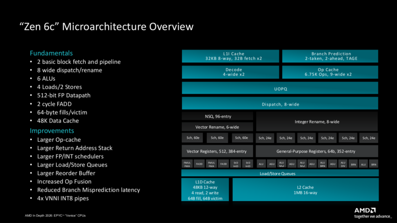
The big takeaway here is that AMD is making a big push here for architectural efficiency at the CPU core level rather than adding a ton of new hardware resources to the core. Which is not to say that AMD is not investing a great deal more transistors in the core, thanks in big part to TSMC’s 2nm process node, but we are not looking at a wider decoder, an array of new compute pipelines in the backend, or such. Instead, the emphasis is generally around making changes to keep all of that hardware better fed, or to help it extract IPC from a larger window of instructions.
This is efficiently enumerated on AMD’s own list of improvements on their slides. A larger Op-cache, a larger return address stack, a larger FP/INT scheduler, and more. It is actually quite remarkable that AMD is hitting such significant IPC gains for how little of the core compute hardware has been overhauled.
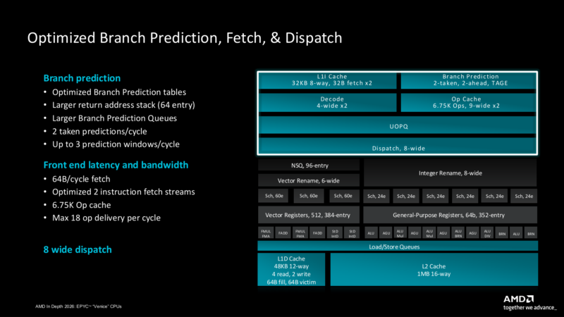
Taking a look at the front-end of the microarchitecture, AMD has retained their 8 wide setup. A pair of 4-wide decode blocks eventually works its way through to feed an 8-wide dispatch unit. The branch prediction unit itself has not grown in size (the number of predictions it can make), standing at 3 predicts and 2 takes per cycle, but AMD has optimized it. The return address stack has gone from 52 to 64 addresses, and the overall queue size for the branch predictor is larger.
Meanwhile the operation cache has been enlarged for Zen 6 in a couple of different ways. The overall cache size has gone from 6K instructions to 6.75K (~13% larger). And AMD has improved the bandwidth in the op cache as well to better match its size; the former 2×6-wide unit is now a 2×9-wide unit, allowing the CPU to deliver up to 18 operations out of the cache per cycle.
Zen 6 Mid-end
Moving on to AMD’s scheduler, this is where things get more interesting for the Zen 6 microarchitecture. While falling short of a radical alteration, AMD has given the scheduling of integer instructions a lot of thought here.
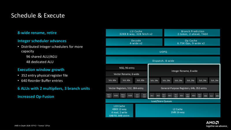
With dispatch coming out of the CPU’s front-end still being 8 wide, the integer renaming unit in the CPU similarly stands pat at 8 instructions wide. But AMD’s formerly unified scheduler has been broken up into 6 24 entry units, with AMD now employing a distributed strategy for instruction scheduling. Notably, these 6 schedulers are not all identical, either: 2 of them (48 entries) are dedicated to asthmatic (ALU) operations, while the remaining 4 (96 entries) are shared between math and address generation (AGU) operations. The is juxtaposed to Zen 5, which had a fixed 56 entry AGU schedule and a fixed 88 entry ALU scheduler.
The net impact of this change is that while Zen 6 loses any kind of dedicated AGU scheduler, ALU scheduling can now be distributed over the entire array of scheduling units if needed. Conversely, however, fewer slots are dedicated to ALU operations overall, allowing AGU scheduling to take over the bulk of the scheduling window when that is most optimal. It is a change that is rooted in not only giving Zen 6 the ability to schedule more instructions, but to be more flexible in how it does so, so that less hardware is left idle.
Scheduling aside, the rest of the execution window has been expanded as well. Zen 6 is taking the reorder buffer (ROB) from 448 entries to 640 entries, a 43% improvement there in order to extract more parallelism from an instruction stream by looking over a longer number of instructions. Meanwhile instructions will be competing less for physical registers, as the physical register file is going from 240 registers to 352, a 47% size increase.
According to AMD, the company has also made changes to increase how often that the CPU core can fuse operations together. Though the company has not specified just what those changes entail.
Otherwise, the floating point side of the core has not been left out, either. While still using a trio of instruction schedulers there, placed behind a 6-wide rename unit, those schedulers now hold 60 entries, up from 32 per on Zen 5.
Zen 6 Backend
And while AMD has not added any new pipelines to the Zen 6 CPU backend, they have made a few different tweaks to handle what kinds of instructions each pipeline can take.
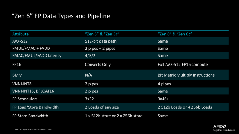
On the AVX/AI front, 4 of the ALU pipes can now take VNNI-INT 8 instructions, which doubles the number of capable pipes from Zen 5. Notably, however, the number of INT16 and BF16-capaable pipes remains unchanged at 2, so this is very much an INT8-focused improvement.
Meanwhile, nothing has changed with regards to the more fundamental aspects of the backend pipelines, including the number of pipes for basic fused instructions or their latency.
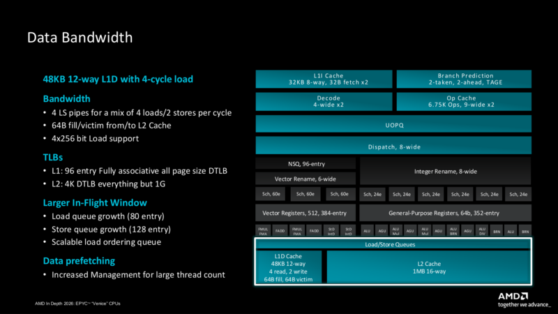
Finally, feeding all of the pipes in the CPU backend is an even more capable set of load/store units and TLBs. AMD has kept their 4 load/store pipes here, which can handle up to 4 loads or 2 stores per cycle. Of note here, while the load/store units could only do 2 FP loads per cycle on Zen 5, that has been modestly enhanced for Zen 6; the L/S units can now do 4 loads in a cycle if they are smaller 256-bit loads. Otherwise, the total cap remains at 1024-bits per cycle, as it was on Zen 5 when doing 512-bit loads (2×512).
The queues for the load/store units have also been enlarged once again. Coming from Zen 5’s 64 entry load queue, for Zen 6 it is now 80 entries. And the store queue has gone from 104 entries to 128 entries.
Elsewhere, the L1 data cache remains unchanged from Zen 5. This means we are looking at a 48KB, 12-way cache, with a 4 cycle latency for loads.
What is not represented in the facts and figures here is AMD’s broader effort to manage data prefetching. The company has tweaked the Zen microarchitecture to better handle large thread counts, having invested what we are told is a lot of resources into improving data prefetching. So the data feeding improvements extend just beyond how big the load/store queues are; what is going into them has also been considered.
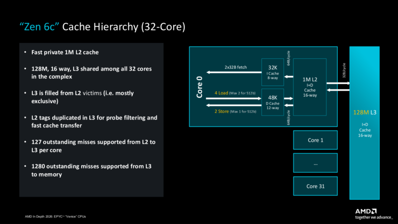
Speaking of caches, here is an overview of Zen 6’s cache hierarchy. Like the load/store changes, there are not any wild changes here, as the amount of bandwidth between various levels of the cache remains unchanged versus Zen 5. The L1 caches can fill at 64B/cycle, while the L2 cache fills from the L3 at 32B/cycle.
The large size of the L3 cache on Zen 6c CCDs is something that, if you will pardon the pun, is a big deal for AMD. Whereas Zen5c CCDs only had 32MB of L3 cache for 16 CPU cores – or 2MB of L3 per core – Zen 6c takes that to 128MB of L3. Even with the fact that this L3 cache now needs to support a much larger array of 32 cores, the over-5x increase in L3 cache size means that there is now 4MB of L3 cache per CPU core. This removes one of the only non-frequency differences between AMD’s big and compact CPU cores.
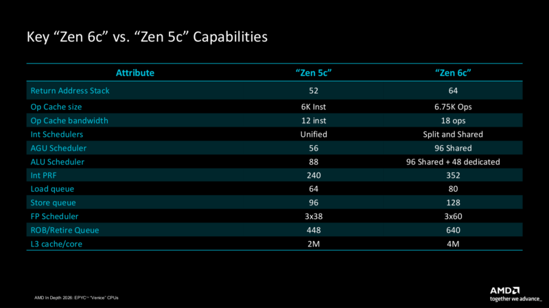
Wrapping up our look at what’s new in the Zen 6 microarchitecture, here is a final table for the more tabularly-minded, outlining some of the major changes to the various caches, buffers, and schedulers on the CPU core.