
Bringing Zen 6 Together: Venice I/O Die and Socket SP7
Moving beyond the Zen 6 architecture and the individual CCDs, let us talk about the other pieces of silicon that make up a complete Venice chip: the I/O Dies.
As has been the cast for the past several generations of the Zen architecture, AMD relies on separate chiplets for the CPU cores and then the uncore – everything that is not the CPU core complexes – which falls under the domain of the IOD. That includes the memory controllers, PCIe controllers, security processor/root of trust, and the Infinity Fabric (XGMI) link for a dedicated backhaul to AMD’s server-grade GPUs. In other words, it is home to all of the I/O that feeds AMD’s CPU cores.
In some respects, the IOD in Venice is one of the biggest overhauls coming from the Zen 5-based Turin family. While AMD has not changed the IOD paradigm, they have developed a completely new IOD that is built on TSMC’s 6nm process node. As a result, Venice is rolling out with a slew of new technologies to provide AMD’s new Zen 6 CPU cores with all the I/O they can handle.
SP7 IOD: It Takes Two
Since today is the launch of the Venice SP7 platform, we will start our look at the Venice IOD with the SP7 version of it.
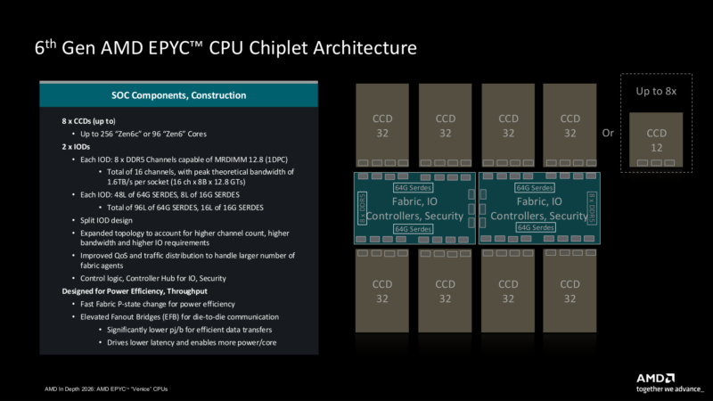
The most obvious change here is that AMD has split the IOD into two. Rather than having one large, monolithic IOD per server CPU, AMD now employs two smaller IODs. Each IOD in turn contains half of the chip’s memory channels, PCIe lanes, and CCD connections. In theory, this gives AMD some flexibility down the line to develop smaller EPYC chips with less I/O (e.g. the 8006 series), but for now all SP7 CPUs come with two IODs.
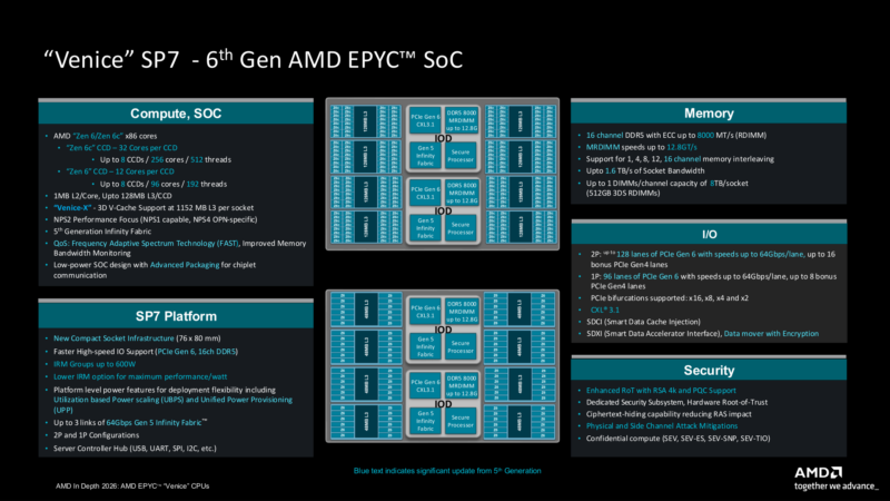
Compared to Turin’s IOD, the biggest change with the Venice SP7 IOD are its memory improvements. While the industry as a whole is still on DDR5 memory technologies, AMD has built a much stronger and faster memory controller for Venice. The new IOD can support 8 channels of DDR5 running at up to 8000 MT/sec, or, faster still, second generation MRDIMMs running at 12800 MT/sec. This marks the first platform from AMD to support MRDIMMs, and coming from Turin effectively doubles the amount of memory bandwidth available per channel.
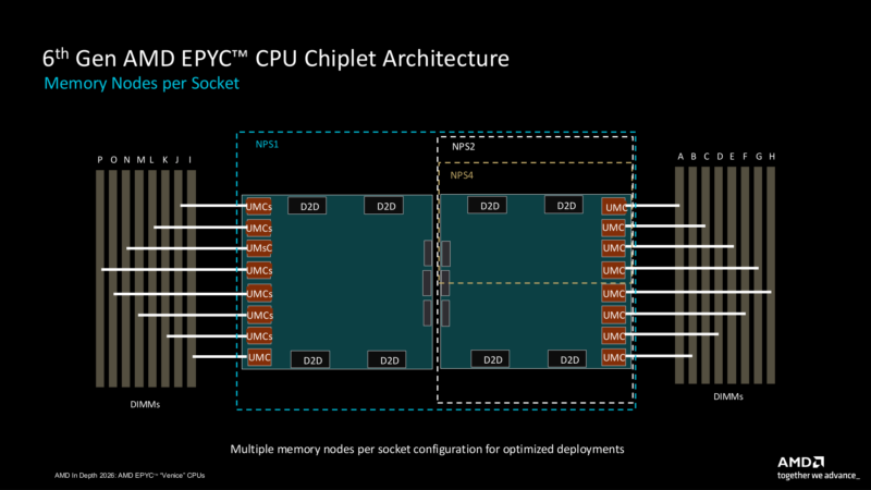
With two IODs on a chip, this gives a single Venice SP7 CPU a total of 16 memory channels. Which, in their fastest configuration, amounts to 1.6TB/second of bandwidth for a single CPU. Or in terms of capacity, a single socket can be paired with up to 8TB of memory. Do note, however, that AMD is only supporting 1 DIMM per channel here; so 32 DIMM configurations are off the table for Venice SP7.
Meanwhile, as we noted a bit earlier, the total number of CCDs that an IOD can support has changed with this generation. Instead of Turin’s ability to host 16 CCDs, Venice IOD brings that down to 4 per IOD, for a total of 8 CCDs on a single CPU. Accordingly, AMD has boosted the speed of the data path between the IODs and CCDs to keep up with the larger number of CPU cores. In particular, there is still one SDP port for at most every 8 CPU cores. Each port offers 32 bytes/cycle of bandwidth.
In briefing us on Venice, AMD’s engineers noted that the sheer number of cores and the amount of bandwidth needed to feed them is part of the reason that AMD went with the dual IOD design this time around.
As for external devices, the new IOD brings with it a major upgrade to I/O bandwidth with the inclusion of PCIe gen6 and CXL 3.1 support. The latest and greatest generation of PCIe technology marks an extensive overhaul of how PCIe works under the hood, ditching classic NRZ encoding for a combination of PAM-4 encoding with forward error correction. The change is designed to stave off the constant growth of PCIe’s signal bandwidth needs, trading even higher frequencies there for a more complex signaling method.
A single Venice SP7 IOD is equipped with 48 64G SERDES, which are what is used to drive the updated PCIe lanes, along with another 8 16G SERDES for other communications. This gives us our final limit for an SP7 chip of 64 lanes of PCIe Gen6/CXL 3.1 comms, as well as 8 “bonus” lanes of PCIe Gen4 for other needs.
Finally, with all of the changes to both the CCDs and IODs, AMD has also significantly upgraded the packaging used to connect everything. AMD has finally moved past using classic 2D organic substrates here for a mix of elevated fan-out bridges and silicon bridges.
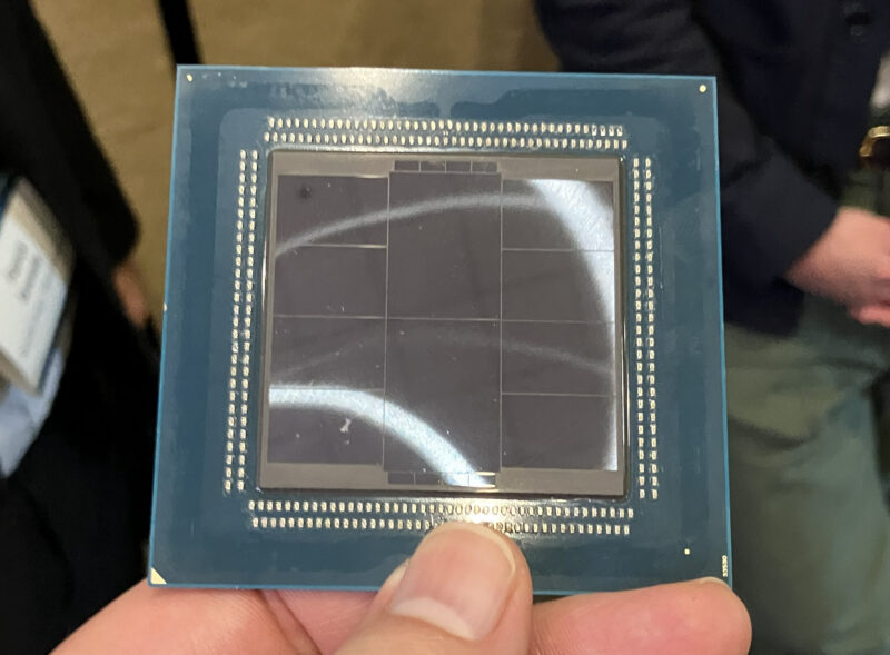
Specifically, the IODs are now connected to the CCDs via small silicon bridges (TSMC’s version of EMIB) which is why the CCDs are now placed directly next to the IOD. Placing the dies closes and routing the signals through a silicon interposer has allowed AMD to significantly cut down on the amount of energy (on a pico-joules per bit basis) used to move data between the dies. Furthermore, this also cuts down on latency through both the reduced distance and the faster interconnect.
The trade-off, of course, is that this makes Venice the most complicated EPYC chip yet from a packaging perspective. While still a step below AMD’s most complex chips like the Instinct MI455X, which uses die-to-die bonding on top of everything else, it still requires AMD to spend more on packaging overall and to tap into their limited supply of advanced packaging facilities in order to build the chip.
SP8 IOD: Fewer Memory Channels, More PCIe Lanes
Very briefly here, we will also take a look at the IOD design that AMD is using for Venice SP8. That platform does not launch until next year, but the company is releasing the technical info for its IOD alongside the SP7 IOD.
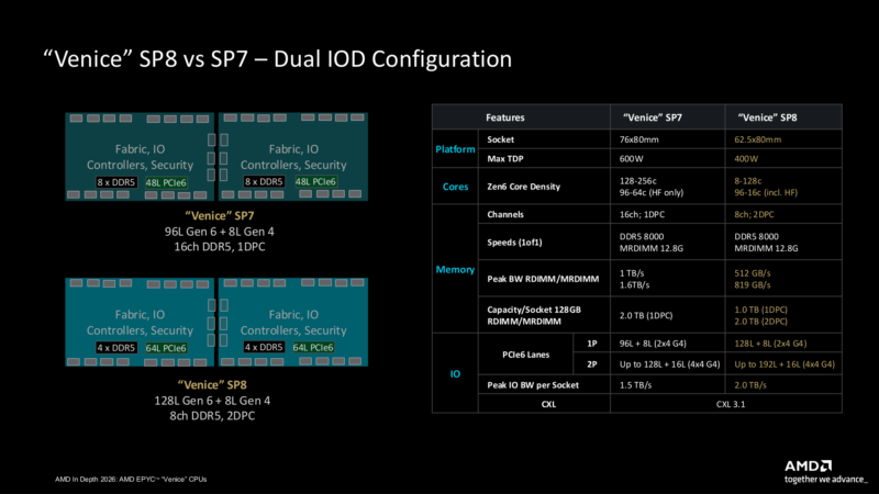
At a high level, Venice SP8 is getting its own IOD. AMD is not just recycling the SP7 IOD here, but instead has produced a separate and smaller IOD specifically for use in Venice SP8. And, despite the smaller size, AMD has kept the dual IOD structure.
The big takeaway here is that the Venice SP8 IOD is in effect an IOD with less of an emphasis on memory bandwidth and more of an emphasis on external I/O bandwidth.
In terms of memory bandwidth, Venice SP8 drops down to 8 channels of DDR5 instead of 16 channels, effectively halving its memory bandwidth. It does retain all of the same memory features as Venice SP7, however, including support for DDR5-8000 RDIMMs and DDR5-12800 MRDIMMs, so the latest memory technologies have been retained. And, because of the smaller number of memory channels, it has been qualified to support 2 DPC, allowing for a Venice SP8 chip to be paired with up to 16 DIMMs – or just as much memory as a Venice SP7 chip.
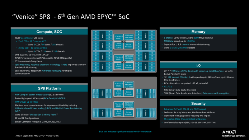
What Venice SP8 loses in memory bandwidth it makes up for in PCIe lanes. Each Venice SP8 IOD offers 64 lanes of PCIe Gen6/CXL 3.1, allowing for 128 lanes in total in a 1S configuration. This is a further 32 lanes (2 root ports) more than Venice SP7.