
SP7 Platform Topologies: One or Two Sockets, Many Configurations
Going up one final level, let us take a look at how everything comes together to make a Venice chip. As before, we will start with a look at the SP7 platform, which is AMD’s flagship platform for Venice.
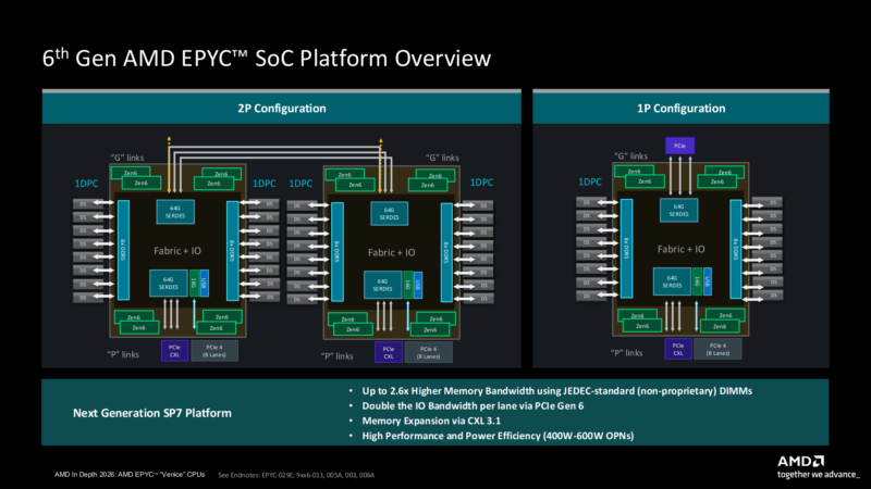
Venice SP7 can be operated as either a single socket configuration or in a dual socket configuration. As with Turin before it, going dual-socket means sacrificing some of the PCIe lanes from each CPU, as those are repurposed as xGMI lanes for the I/O needed to connect the two CPUs.
Binding two chips together in this fashion typically consumes 32 PCIe lanes from each chip, leaving 128 lanes of PCIe Gen6 (64 per CPU) for general purpose I/O to other devices.
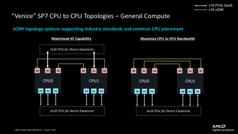
However, as a secondary option, system builders can opt to route even more bandwidth between the Venice SP7 chips, sacrificing a third set of 16 lanes (i.e. a third root port) in order to further increase the amount of bandwidth between the two CPUs. This allows for the equivalent of 48 lanes of PCIe/xGMI going between the CPUs, leaving 96 lanes (48 per CPU) for general I/O.
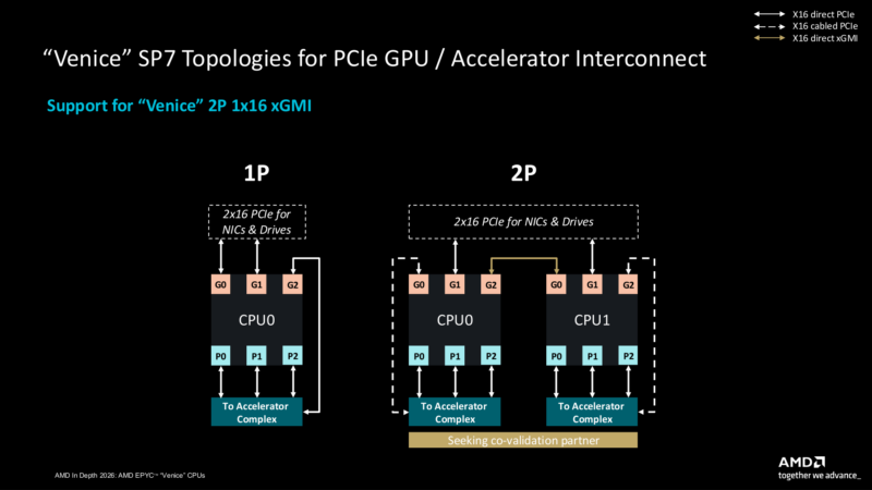
Meanwhile AMD has yet another set of topology options for driving a GPU or other accelerator. In a 2P configuration the CPU-to-CPU link can drop down to just 16 lanes (1 root port), freeing up as much I/O bandwidth as possible to go to the accelerators. In this case, 128 lanes would be allocated to the GPU, while another 32 lanes are available for networking and storage.
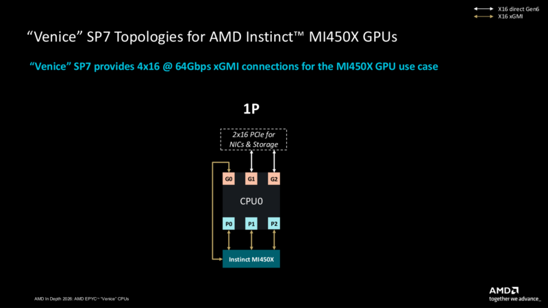
And AMD themselves uses a variation of this for their Helios rackscale systems, which are optimized for GPU performance. With a single Venice SP7 CPU as a host, 64 lanes are set to xGMI mode and allocated to the Instinct MI450X accelerator. That leaves another 32 lanes for networking and I/O.
Ultimately, it is up to each system builder to decide how they want to go about allocating the lanes within a Venice system. This is a decision that is baked into the motherboard itself –outright deciding where to physically route the lanes coming from the CPU sockets – so the distinction between a CPU server and a GPU server is quite important here.