

AMD EPYC 9006 SP7: Flagship Venice
Leading the charge in AMD’s Zen 6-based server CPU lineup is the full/high-performance Venice platform, which AMD is currently calling EPYC 9006 SP7. Named after the socket it pairs with, the new socket SP7, EPYC 9006 SP7 is the direct successor to AMD’s EPYC 9005 Turin and Turin Dense processors.
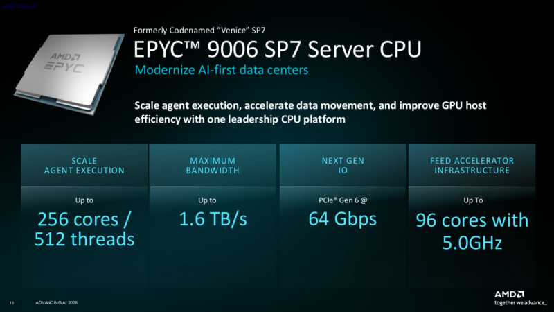
The EPYC 9005 series covered a very wide span of processors that included both high-frequency chips and high-core-count chips, and the 9006 SP7 platform will do the same. The highest density EPYC 9006 SP7 chips will feature up to 256 Zen 6c cores. Meanwhile, the highest performance chips will feature up to 96 Zen 6 cores.
Regardless of the core configuration, all SP7 chips announced so far feature the same memory support, with 16 channels of DDR5 and support for both RDIMMs and MRDIMMs. So AMD is not engaging in any kind of tiering here to limit high-end memory support to certain SKUs.
All of the SP7 SKUs can be used in a 1P or 2P configuration. However, in a 1P configuration, they support only 96 PCIe lanes, down from 128 lanes in the equivalent Turin processors. Consequently, there seem to be some compromises coming from the Turin generation.
| AMD EPYC 9006 SP7 SKUs | ||||||
| CPU Cores | Threads | Max Boost Clock | Base Clock | L3 Cache | TDP | |
| AMD EPYC 9996 | 256 | 512 | 4.1 GHz | 2.55 GHz | 1024 MB | 600W |
| AMD EPYC 9966 | 192 | 384 | 4 GHz | 2.9 GHz | 768 MB | 600W |
| AMD EPYC 9846 | 168 | 336 | 3.7 GHz | 2.85 GHz | 768 MB | 500W |
| AMD EPYC 9756 | 128 | 256 | 4 GHz | 3.15 GHz | 512 MB | 500W |
| AMD EPYC 9G76 | 96 | 192 | 4.8 GHz | 3.4 GHz | 384 MB | 500W |
| AMD EPYC 9656 | 96 | 192 | 3.7 GHz | 3.05 GHz | 512 MB | 400W |
| AMD EPYC 9686F | 96 | 192 | 5 GHz | 3.4 GHz | 384 MB | 500W |
| AMD EPYC 9556 | 64 | 128 | 4.3 GHz | 2.75 GHz | 384 MB | 300W |
| AMD EPYC 9586F | 64 | 128 | 5 GHz | 3.75 GHz | 384 MB | 500W |
Finally, in terms of market positioning, AMD considers SP7 to be their flagship platform for their Zen 6 server processors, as this is the platform for both their high-density and high-performance offerings. These are the chips that AMD will be pitching for both server host nodes with the high-frequency chips, and for use in agentic AI servers with the high-core-count chips.
A fun one for longtime STH readers, and that is cache. In 2021 we highlighted how server processors were heading towards the GB era of onboard cache. While we have seen that in specific 3D V-Cache SKUs, but it is now in the mainstream EPYC 9996 CPU.
The AMD EPYC 9006 SP7 will also be the first chip family out of the fabs for AMD. With these chips also forming the backbone of AMD’s Helios rackscale systems, AMD will ship the SP7 chips first, with AMD set to release them in Q4 of this year. Given the expected ramp-up period (in part because TSMC will continue bringing more 2nm capacity online), it is not yet clear how much of AMD’s EPYC 9006 SP7 supply will reach the market as loose chips versus going into Helios racks. Helios does need “perfect” chips, which, coupled with the system’s cost, means that Helios cannot consume all of AMD’s Venice production. For now, how AMD is splitting its early 2nm wafer is a secret that stays inside the halls of AMD’s headquarters.
AMD EPYC 9006 SP8: Mid-Tier Venice
As with the Zen 5 generation, AMD is going to be offering its server chips over multiple platforms/sockets. Joining EPYC 9006 SP7 next year will be its mid-tier counterpart, EPYC 9006 SP8. This is where AMD makes substantial changes to how it organizes and names its server chip platforms.
AMD EPYC 9006 SP8 can in some ways be seen as a successor to Sorano, AMD’s mid-tier EPYC processors. Besides getting its own codename within AMD’s hierarchy, Sorano and its predecessors were also sold under their own EPYC 8xxx branding, differentiating them from the flagship EPYC 9xxx processors. There is no obvious suffix or other tell in the part number to indicate whether it is a SP7 or SP8, but the EPYC 9006 series clearly targets specific market segments.
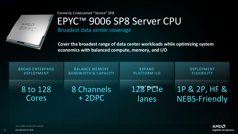
Naming qualms aside, the EPYC 9006 SP8 chip family will serve as AMD’s more value-oriented chip offering. Rather than offering the performance extremes of the SP7 chips, the SP8 chips will offer more moderate performance for lower motherboard and chip costs.
Hardware-wise, the Venice SP8 chips are effectively half as EPYC as the Venice SP7 chips. The maximum CPU core count is 128 cores versus SP7’s 256 cores, and there are 8 channels of DDR5 memory instead of 16.
As with the rest of the Venice lineup, AMD has not distributed any detailed architectural information on the platform. But in a single enhanced photo of the Venice chips with die shots superimposed, AMD shows off a couple of slightly smaller EPYC chips, some with as few as four CCDs. Notably, these chips seem to also feature two IODs, but these IODs sport a different floorplan than the IODs used in the SP7 chips.
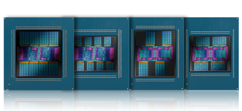
The full ramifications remain to be seen, but the implication is that the EPYC 9006 SP8 family will not simply be EPYC chips with half as many chiplets.
We will also see AMD mixing Zen 6 and Zen 6c chiplets in this product line. With core counts as high as 128 and frequencies as high as 5.0GHz, AMD will need both kinds of chiplets to flesh out the product lineup.
Meanwhile, one advantage that the SP8 chips will have over their SP7 brethren is the number of PCIe lanes. Whereas the SP7 chips all have 96 available PCIe 6.0 lanes, the SP8 chips all come with 128 lanes. Consequently, it seems the EPYC 9006 SP8 family is being positioned as the better processor for customers who need extra I/O bandwidth over additional memory bandwidth or CPU cores.
Speaking of memory bandwidth, all of the chips announced so far are listed as supporting the same memory capabilities: eight RDIMMs at up to DDR5-8000 or eight MRDIMMs at up to DDR5-12800. Which means that MRDIMM support is seemingly going to be available at every level of the Venice platform, right on down to the itty-bitty EPYC 9016, an 8 CPU core part. Notably, SP8 is also the only platform AMD has explicitly confirmed supports 2 DPC. Not that we expected it for SP7, but customers who need a large amount of memory can fill 16 DIMMs on Venice SP8 just as they can on Venice SP7.
| AMD EPYC 9006 SP8 SKUs | ||||||
| CPU Cores | Threads | Max Boost Clock | Base Clock | L3 Cache | TDP | |
| AMD EPYC 9746 | 128 | 256 | 4 GHz | 2.9 GHz | 512 MB | 400W |
| AMD EPYC 9736P | 128 | 256 | 3.7 GHz | 2.7 GHz | 256 MB | 360W |
| AMD EPYC 9736 | 128 | 256 | 3.7 GHz | 2.7 GHz | 256 MB | 360W |
| AMD EPYC 9676F | 96 | 192 | 5 GHz | 3.1 GHz | 384 MB | 400W |
| AMD EPYC 9646P | 96 | 192 | 3.7 GHz | 2.8 GHz | 256 MB | 300W |
| AMD EPYC 9646 | 96 | 192 | 3.7 GHz | 2.8 GHz | 256 MB | 300W |
| AMD EPYC 9576F | 64 | 128 | 5 GHz | 3.55 GHz | 384 MB | 400W |
| AMD EPYC 9536P | 64 | 128 | 4 GHz | 3.25 GHz | 256 MB | 300W |
| AMD EPYC 9536 | 64 | 128 | 4 GHz | 3.25 GHz | 256 MB | 300W |
| AMD EPYC 9526 | 64 | 128 | 3.7 GHz | 2.75 GHz | 256 MB | 220W |
| AMD EPYC 9476F | 48 | 96 | 5 GHz | 3.65 GHz | 192 MB | 330W |
| AMD EPYC 9456P | 48 | 96 | 3.7 GHz | 3.2 GHz | 256 MB | 265W |
| AMD EPYC 9456 | 48 | 96 | 3.7 GHz | 3.2 GHz | 256 MB | 265W |
| AMD EPYC 9376F | 32 | 64 | 5 GHz | 3.8 GHz | 192 MB | 285W |
| AMD EPYC 9356P | 32 | 64 | 4.5 GHz | 3.6 GHz | 192 MB | 250W |
| AMD EPYC 9356 | 32 | 64 | 4.5 GHz | 3.6 GHz | 192 MB | 250W |
| AMD EPYC 9336 | 32 | 64 | 3.7 GHz | 3.15 GHz | 128 MB | 195W |
| AMD EPYC 9276F | 24 | 48 | 5 GHz | 3.8 GHz | 96 MB | 230W |
| AMD EPYC 9256 | 24 | 48 | 4.5 GHz | 2.85 GHz | 96 MB | 190W |
| AMD EPYC 9176F | 16 | 32 | 5 GHz | 3.9 GHz | 192 MB | 200W |
| AMD EPYC 9116 | 16 | 32 | 4.5 GHz | 2.85 GHz | 48 MB | 160W |
| AMD EPYC 9016 | 8 | 16 | 4.8 GHz | 3.05 GHz | 48 MB | 130W |
That small core count also underscores the size of the EPYC 9006 SP8 product stack: AMD has announced 22 Venice SP8 SKUs, versus just 9 SKUs for the EPYC 9006 SP7. The high-end chips will only scale down to 64 cores, whereas over half of the SP8 stack features 48 CPU cores or fewer. The much deeper chip stack means much more variety overall, particularly since AMD supports 2P operation on some chips in this generation, something Sorano lacked. Consequently, there are chip variations, such as chips limited to 1P operation (P-suffix) and chips with a massive amount of L3 cache relative to the CPU core counts.
Finally, with lower core counts and fewer memory channels, EPYC 9006 SP8 chip TDPs will be a bit lower. The most powerful chips will top out at 400W, which is two-thirds the TDP of the biggest SP7 chips. On the other hand, that is almost twice the TDP of the hottest Sorano chip, so AMD’s mid-tier EPYC platform will look very different.
In any case, EPYC 9006 SP8 will be the second family of 6th-generation EPYC chips AMD will release. The company will begin shipping these chips in the first half of next year.

“AMD will be adding AI compute extensions, which they are calling ACE. Presumably, these will be something akin to Intel’s AMX or Arm’s SME”
I’m surprised at this statement. We know exactly what ACE is since its whitepaper is half a year old, and compiler enablement is well underway for both GCC and LLVM. It could be a nice article to explain it here though.