

AMD EPYC 9006X SP7: Venice-X Marks the Return of 3D V-Cache
Looking a bit farther down AMD’s EPYC timeline, the company is also roadmapping a third Venice variation specifically aimed at the HPC market. Dubbed Venice-X, these chips will mark the return of AMD’s stacked 3D V-cache to enable the company to produce server CPUs with a massive amount of L3 cache per CPU core.
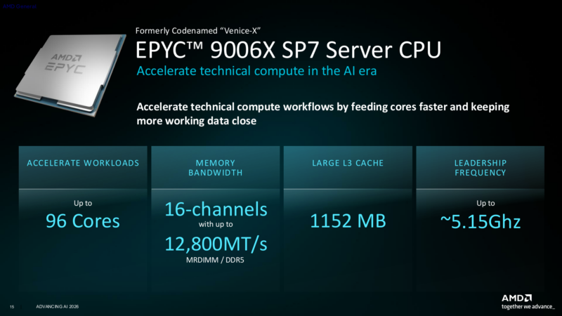
With Venice-X not slated to become available until some point in the second half of 2027, potentially over a year from now, AMD is releasing fewer details here. At a high level, the big news is that these high cache chips will use the SP7 socket/platform, and will be made from Zen 6 chiplets with additional L3 cache.
The fastest chips will feature up to 96 CPU cores, while AMD expects peak clock speeds near 5.15GHz, about 150MHz (~3%) faster than the peak Venice SP7 chips. As for the L3 cache, Venice-X chips will feature up to 1152MB of L3 cache, versus the 384MB found on the regular SP7 Zen 6 chips. This works out to 12MB of L3 cache per CPU core in a full configuration, and potentially more on any chips with a cut-down number of enabled CPU cores.
However, while Venice-X chips will carry the banner as the EPYC chips with the most L3 cache in total, it will not be a massive lead in this generation. The densest Zen 6c-based Venice SP7 chips will offer as much as 1024MB of L3 cache (and without using cache stacking), and as a result, Venice-X’s place in the world will be less about the total amount of L3 cache, and more about how much cache is available to the high-frequency Zen 6 CPU cores.
Overall, Venice-X marks the return of AMD’s 3D cache stacking technology to its server CPU lineup after being absent in the EPYC 9005 generation. As we learned when AMD skipped it in the last generation, the market for server chips with additional physical cache is less certain than it is in the consumer market (where AMD has seen a lot of success with the Ryzen X3D chips), and this may be why AMD is taking a more focused approach on HPC with Venice-X. Still, with the chips so far out, AMD has plenty of time to adjust its product positioning well before anything launches.
L3 cache aside, Venice-X will support the full feature set of the SP7 platform. Most notably, this means supporting the same 16-channel memory architecture with MRDIMM support, so those large cache chips will be backed by substantial memory bandwidth.
AMD will undoubtedly have more details on Venice-X as we get closer to the chips’ release. But for now, we will need to wait for them to launch in the second half of next year.
AMD EPYC 9006 LP: Verano Brings LPDDR5X Support to EPYC
The final EPYC 9006 chip recently announced may also be the most interesting, and that is Verano.
A name we have seen AMD kicking around for over a year as part of its future rack-scale system plans, Verano sits somewhere between a side project and a successor to Venice. The Zen 6 architecture chips are not being placed under the Venice codename, and for good reason: they are a rather distinct product compared to the Venice SP7 and SP8 chips.
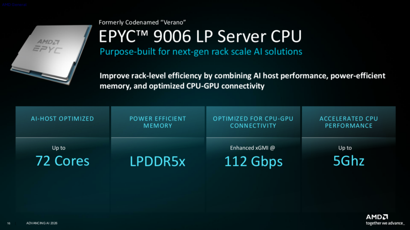
At a high level, AMD is targeting these chips particularly at the AI market as a host processor for GPU clusters. To accomplish this, AMD is designing a Zen 6-based EPYC chip with several key improvements that set it apart from Venice and make it look a bit more like rival NVIDIA’s CPUs, which are now in the STH lab.
The big change, of course, is LPDDR5X support. According to AMD, the switch to low-power memory brings two benefits. The first is power consumption. Per byte of memory and per byte of memory bandwidth, LPDDR5X consumes less energy than DDR5. The second benefit is memory bandwidth. Verano will support 24 channels of LPDDR5X, versus 16 channels on Venice SP7.
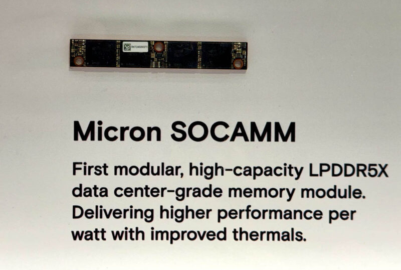
At this point, AMD is not disclosing what memory frequencies the EPYC 9006 LP chips will support. But the LP platform will use SOCAMM2 modules to allow for removable/upgradable/serviceable memory, similar to other high-end server CPUs set to be released over the next year.
The EPYC 9006 LP chips will also feature a much more modest core count of just 72 CPU cores. With peak clock speeds of up to 5GHz, these will seemingly be Zen 6 cores (rather than Zen 6c), with AMD favoring efficiency versus dense compute throughput.
But the real killer feature for AMD’s plans is Verano’s support for a faster xGMI interface, which, as we discussed earlier, is the physical interface AMD uses to connect its EPYC CPUs to each other in multi-processor configurations, as well as to its Instinct GPUs. Verano can run its xGMI link at up to 112Gbps, just shy of twice as fast as EPYC 9006 SP7’s 64Gbps links.
The particularly interesting implementation tidbit here is that AMD’s xGMI links have been closely related to PCIe specifications throughout their lifecycle. AMD EPYC 9005 has a 32Gbps PCIe Gen5-class link, EPYC 9006 has a 64Gbps PCIe Gen6-class link, and Verano will surpass that. As a result, AMD is finally moving a bit ahead of PCIe in per-lane bandwidth, and depending on the technical decisions AMD makes to get there, we may be looking at AMD going on a track to decouple from it entirely. PAM4 112G is all over modern AI data centers today, so it seems like more than a coincidence.
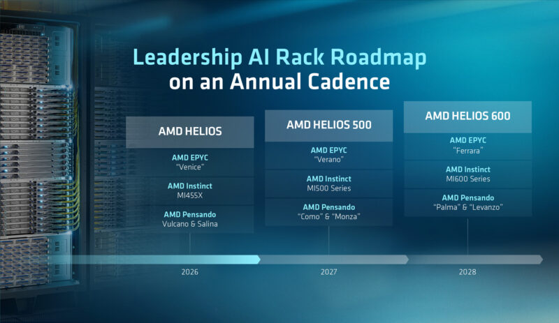
This new link, in turn, would go hand-in-hand with AMD’s future generation of Instinct accelerators, the MI500 series, which would also implement the newest xGMI interconnect. The two chip families are major components of AMD’s future rack-scale system, currently called Helios 500, making Verano a key part of AMD’s product plans. This will not be just a Zen 6 server chip with a different type of memory.
Reading between the lines, AMD is clearly designing an entirely new IOD for this part. Whether they do anything special with the CCDs remains to be seen, though 72 CPU cores neatly divide by the 12 cores we calculate are in each of AMD’s initial Zen 6 CCDs.
To that end, Verano is, for all intents and purposes, a mid-generation kicker of sorts to support AMD’s rackscale system plans. With the firm intending to release new rackscale systems on a yearly cadence to match its Instinct GPU release cadence, but with AMD releasing a new CPU architecture only about every two years, the company will release chip variations such as Verano to fill the schedule gap.
The most exotic of the EPYC CPUs will also be the farthest out. As with Venice-X, Verano is currently slated for a release in the second half of 2027, and given AMD’s Helios delivery plans, it is tough to imagine it being anything other than late in the year. Though only time will tell.


“AMD will be adding AI compute extensions, which they are calling ACE. Presumably, these will be something akin to Intel’s AMX or Arm’s SME”
I’m surprised at this statement. We know exactly what ACE is since its whitepaper is half a year old, and compiler enablement is well underway for both GCC and LLVM. It could be a nice article to explain it here though.