
In this article, we are going to explain why Intel’s Skylake-SP PCIe changes have had an enormous impact on deep learning servers. There are several vendors on the market advertising Skylake-SP “single root” servers that are not single root. With the Intel Xeon E5 generation, each CPU has a single PCIe root. Therefore saying that all GPUs are attached to a CPU was an easy way of determining if a server was single root or not. That is not the case with Intel Xeon Scalable.
The world of AI/ deep learning training servers is currently centralized around NVIDIA GPU compute architectures. As deep learning training is able to scale beyond a single GPU and into many GPUs, PCIe topology becomes more important. This is especially so if you want to use NVIDIA’s P2P tools for GPU-to-GPU communication. Intel Xeon chips are still the standard for deep learning training servers. With the Intel Skylake-SP generation, Intel increased the number of PCIe lanes available by eight. At the same time, the company’s PCIe controller architecture for deep learning servers made single root servers less feasible. Combined with CPU price increases, this means that Intel Xeon E5 V3/V4 systems are still widely sought after by customers for training servers.
We explored Single Root v Dual Root for Deep Learning GPU to GPU Systems previously, and now we are going to show why the new generation of CPUs creates a problem for the newest architectures.
Noticing Something is Different with Skylake-SP Single Root PCIe Servers
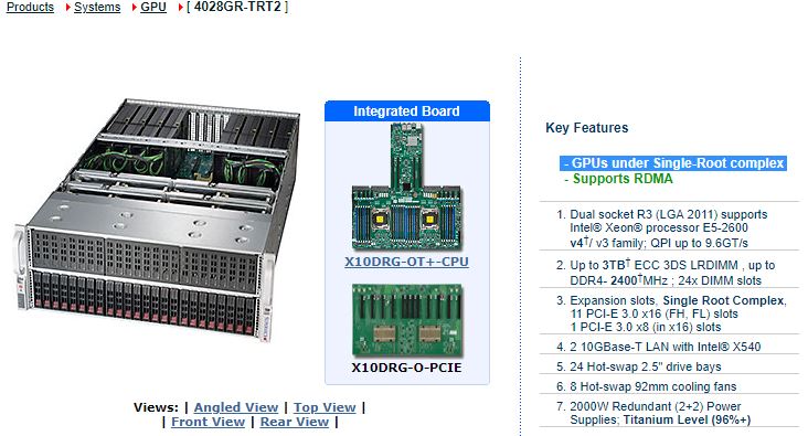
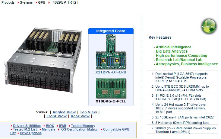
The Intel Xeon Scalable generation has been out for over a year. With the Skylake-SP launch, something strange happened. The number of single root deep learning training servers has plummeted. In the Silicon Valley, the Supermicro SYS-4028GR-TRT2 is perhaps one of the most popular deep learning training platforms we see in local data centers, yet the successor SYS-4029GP-TRT2 has been less popular. We covered the former in our DeepLearning11: 10x NVIDIA GTX 1080 Ti Single Root Deep Learning Server (Part 1) article.
When we looked at the next-generation, we noticed that the “4029” Skylake-SP version did not advertise that all GPUs would be under a single PCIe root complex. Here is a link to both:
- Intel Xeon E5 V3/ V4: Supermicro SYS-4028GR-TRT2
- Intel Xeon Scalable: Supermicro SYS-4029GP-TRT2
Supermicro uses large riser platforms to host the PLX PCIe switches and PCIe slots for GPUs to plug into. Both the Intel Xeon E5-2600 V3/ V4 and the Xeon Scalable versions utilize the Supermicro X10DRG-O-PCIE daughter board.
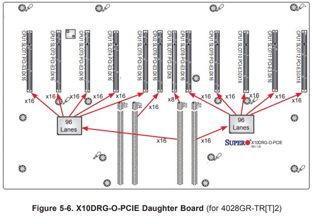
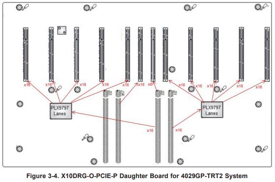
This daughter board takes CPU1 PCIe lanes and pipes them through the PEX PCIe switches. Each switch is the large and expensive 96-97 port PLX model. These switches each utilize 16 ports as a backhaul to CPU1 leaving 80 ports left over for GPUs. With each GPU claiming 16 ports, each of the two PCIe switches can handle five PCIe GPUs. That topology means that in both cases all 10 GPUs are attached to the same CPU.
We knew why the SYS-4028GR-TRT2 is advertised as a single root system:
Conversely, the newer Skylake SYS-4029GR-TRT2 is not:
Being clear, single root PCIe complexes for 8-10 GPUs are a highly sought after configuration for P2P and so the fact that the newer model excludes this language is intriguing. This is not a Supermicro specific or 10x GPU specific concern. Our Tyan Thunder HX GA88-B5631 Server Review 4x GPU in 1U ran into the same limitation due to the new Intel Xeon Scalable architecture.
After speaking to multiple vendors, we found that this is actually a change in the Skylake-SP generation of Intel Xeon Scalable CPUs and it has a big impact. It is also one that the AMD EPYC 7001 cannot remedy.
Getting into this Mesh
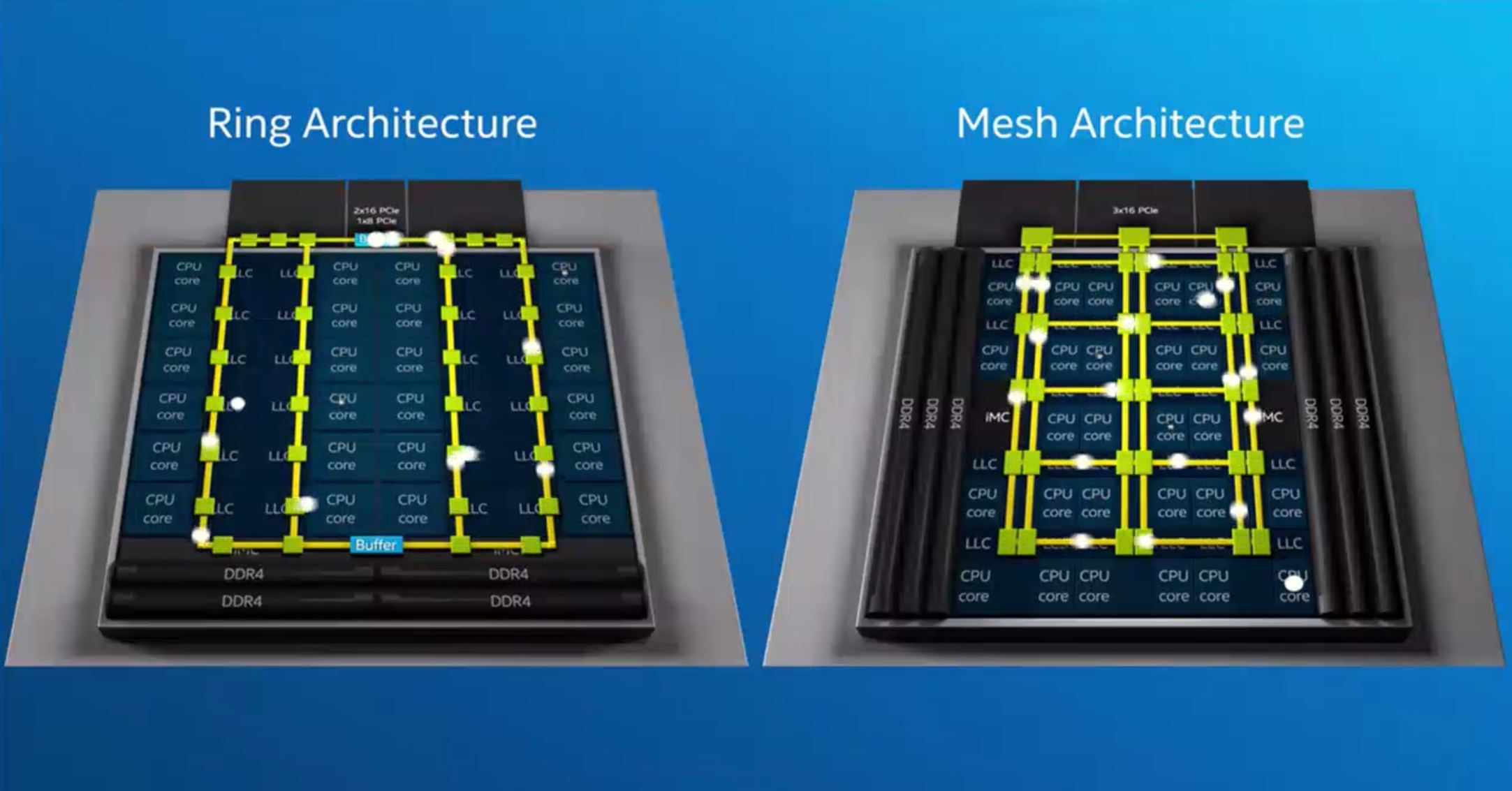
One of the biggest changes with this generation is how the various parts of the Intel Xeon Scalable die are connected. We did an in-depth look at this in our piece: New Intel Mesh Interconnect Architecture and Platform Implications. For our purposes, the key change was moving from the company’s ring architecture to a mesh architecture to support higher core counts.
We actually picked up on the nuance of this change last year but missed the implication. Specifically, what this means to PCIe topology. We focused on this in our first mesh article:
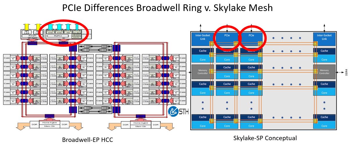
If you look at the Broadwell-EP (Intel Xeon E5-2600 V4) architecture, all of the integrated IO (IIO) is on a single controller in the ring. We are going to use a low-core count example here so you can see the two PCIe x16 and single PCIe x8 controller on the top right ring stop. Single root servers would typically use one of these PCIe 3.0 x16 controllers to connect to a PCIe switch, then connect to half the GPUs. The other PCIe 3.0 x16 controller would connect to another PCIe switch and the other half of the GPUs. Since everything is in a single IIO root, this shared a PCIe root and for deep learning, everything worked well.
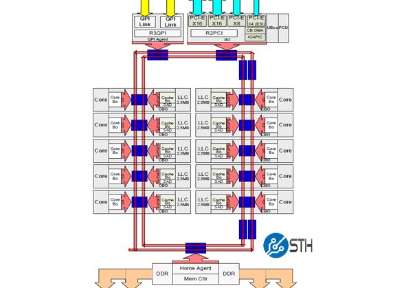
Since there is one IIO component, the industry colloquially equated one CPU to mean one PCIe root. It was this way for four generations of Intel Xeon E5 CPUs.
Now let us take the Intel Skylake-SP 28-core die used on high-end CPUs like the Intel Xeon Platinum 8180 and Xeon Platinum 8176. As you can see there are three external PCIe 3.0 x16 hops atop the mesh. There is a fourth labeled “On Pkg PCIe x16” which can be used for on package components such as Omni-Path “F” series parts. For our purposes, the other three are the ones we are interested in. Note that they all have their own stop on the mesh.
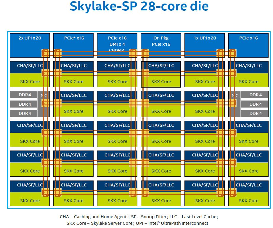
Digging a bit deeper, we can see why these PCIe x16 controllers are different. Here is what the Processor Integrated I/O looks like on the Skylake-SP mesh where you can see that each PCIe 3.0 x16 controller sits on its own mesh stop:
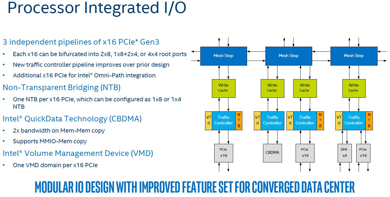
Instead of a single big IIO block, these are split into multiple smaller IIO blocks, each with their own traffic controllers and caches. For deep learning servers, that means that each PCIe x16 controller that is connected to a 96 port PCIe switch and downstream GPUs is on a different mesh interconnect hop. For more technical PCIe enumeration and root complex reasons that we are not going into here, there is an implication. The architecture is not single root like the Intel Xeon E5 generation where all controllers sat in the monolithic IIO ring hop.
Next, we are going to put the pieces together and show how all of this means. We are also going to discuss AMD EPYC Naples and how that can fit into the process. Finally, we are going to give some of our closing thoughts.


 PCIe complexes impacted the ability of the industry to provide single root deep learning and AI servers for the key industry segment)
ASUS has a single root skylake 8 GPU but they’re doing CPU0 > PLX0 > PLX1 so they’re limited to x16 from the diagram like you say https://www.asus.com/us/Commercial-Servers-Workstations/ESC8000-G4/
You’ve got no idea how bad this is for us in the field. It’s ok now since you can still get E5’s but you can’t upgrade to the new gen Xeon Gold and still use P2P.
What this article didn’t talk about enough is that the reason we use single root is to allow inter-GPU traffic. GPU’s talk to each other without having to go back to the CPU.
What is the impact of PLX multi-plexers in the whole system?.
Looking forward to VEGA 20 and NAVI with their own implementation of NVidia’s NVLINK.
What is the impact of 8 vs. 16 PCIe links with current GPU’s like the GTX1080ti (without PLX chips)?
EPYC 2 will support PCIe 4.0 and PCIe 5.0 is on it’s way.
Meanwhile NVidia is laughing it’s but of and people are stupid enough to buy single supply stuff like CUDA, people never learn.
@Lee Chen, thank you. That part was missing for me too, as I had no idea why single root is so important or nice to have.
Hi, very nice work on this artice.
Some other feedback: The “next page” buttons are almost invisible. I saw them only by chance. Consider making them more contrasting.
@Lee Chen
The thing is monolithic architectures are a thing of the past for sever CPUs. The mesh is Intel’s last ditch to keep it alive a litter bit longer but even they will move on to an MCM design sooner than later just like AMD is doing now. If you guys don’t start to adapt your tools to cope with these limitations now, things are just gonna be more painful in a few years. Right now you can still find Broadwell-based CPUs, but you won’t have that option anymore in a few years.
What is the typical CPU utilization of a system like this? Does it even make sense to use Skylake-SP Platinum parts? Does the Xeon D 2xxx have the same issue with PCIe?
This entire discussion is moot because of nvlink. Also what is missing is performance numbers. So what is the effective bandwidth between two gpus on the same plx vs 2 on different plx switches and more importantly the difference in bandwidth between a single root v4 system and the skylake SP one? All the talk means very little without actual performance numbers.
Matt…. you’ve missed the architectural point…. NVLink doesn’t scale using GTX or a large number of RTX GPUs. They’ve got 1080 Ti’s in the top image which don’t use NVLink and are $700 each. If you read their DL10 and DL11 numbers you’ll see, 1080 Ti’s have been the main workhorse of the DL industry since they were released. We use them and all of our competitors use them by the thousands. 2080 Ti’s will replace as prices come down and 1080 Ti’s get harder to source, but it’s a cost thing since you can build 2-3 GTX systems with PCIe instead of 1 Tesla system. V100’s are $9k each which is over a dozen 1080 Ti’s.
We’ve done performance Skylake dual root against E5 single root with 1080 Ti’s at work. Nvidia nccl doesn’t work without single root PCIe on these cards. Skylake’s pcie improvement doesn’t matter here. It varies on model we train, but it’s 20-30% better performance using nccl on E5 single root instead of Skylake dual root.
@Leo Cheng,
@Patrick Kennedy,
Have you checked `nvidia-smi topo -p2p r`, `nvidia-smi topo -m` and the `p2pBandwidthLatencyTest`on a SkyLake like this? (E.g. like Supermicro SYS-4029GR-TRT2?) Is it like this ( https://devtalk.nvidia.com/default/topic/1044817/cuda-setup-and-installation/what-is-the-meaning-of-cns-chipset-not-supported-error-in-nvidia-smi-/post/5301034/#5301034 ) or is it like this ( https://www.servethehome.com/tyan-thunder-hx-ga88-b5631-server-review-4x-gpu-1u/ ) ? Aren’t there any NODE or CNS verdicts?
Supermicro seems to have quietly released a TRT3 variant of the SYS-4029GP, this time with an updated daughterboard (X11DPG-O-PCIE). The manual for the SYS-4029GP-TRT3 has a diagram of the PCIe lanes on page 43, but I’m having some trouble understanding it. By the looks of things, they are using a single x16 PCIe lane from CPU1 feeding a PLX switch that serves 4 PCIe slots at x16, and then another PLX switch in serial that serves 5 more PCIe lanes at x16. From what I gather, that means 9 total GPUs served by a single PCIe root on CPU1. Supermicro still doesn’t advertise single root complex or RDMA support, but is this their answer to that problem? Are they not advertising single root complex because the remaining PCIe slots are not actually on a single root? Any idea how those 5 PCIe lanes hanging off another PLX switch would perform vs the the older daughterboard?
As of September 2019, Supermicro now advertizes both SYS-4029GP-TRT2 and SYS-4029GP-TRT3 as single root complex:
TRT2: “Single Root System for excellent GPU peer to peer communication with sufficient CPU to GPU throughput”
TRT3: “Single Root System, Cascade Mode for maximum GPU peer to peer communication”
“Cascade mode” probably refers to the serial connection through the 2 PLX switches. As for TRT2, it’s unclear to me why they’d advertise it as single root.
Anyhow, does anyone have a performance comparison between single root E5 and Cascade Lake builds on these boards?
The E5 would have to be on a SYS-4028GR-TR2, as the 4029GP systems do not support E5.
The GPUs for the comparison would also ideally be Quadro RTX 6000 or Titan Xp. I just found out that the GeForce cards from the Turing generation (Titan RTX, RTX 2080 Ti…) cannot do P2P at all, so there’s no reason not to use the latest generation of CPUs with them.
Does anyone know if the PCIE backplane is a completely passive device or if it is tightly coupled with the motherboard/motherboard bios?
Could I run the PCIE connector through a ribbon cable back to another mobo with a single epyc 7002 series for example?
I want to set up a machine for LLMs and need a lot of ram since I can’t afford more than ~128GB in VRAM.
I’d like to have all the ram in the system on the same cpu so no intersocket voodoo is occurring and slowing it down.
I really like these PCIE switches for my use case since If I can put a superfast SSD array for temporary storing the model on the GPU side of the switches so I don’t have to traverse the CPU for PCIE access and would be able to do something like mmap the VRAM directly to the SSD array on the fast side of the switch.
This obviously is not as fast as ram but I would have thought the extra cpu cycles I get to skip by bypassing the cpu would make up for it especially if I built the storage array with optane (Expensive but definitely more affordable than a single high vram GPU)
Comments are closed.