Putting it Together
Now we have a few key components. Similar daughterboards are used for the Intel Xeon Scalable Skylake-SP 10x GPU systems by Supermicro and other vendors. We know that the Intel Xeon E5 V3 / V4 generation was advertised as single root while the Skylake-SP version is not. We showed the differences in how the Intel IIO controllers work in each generation. The final step is putting it together into a diagram.
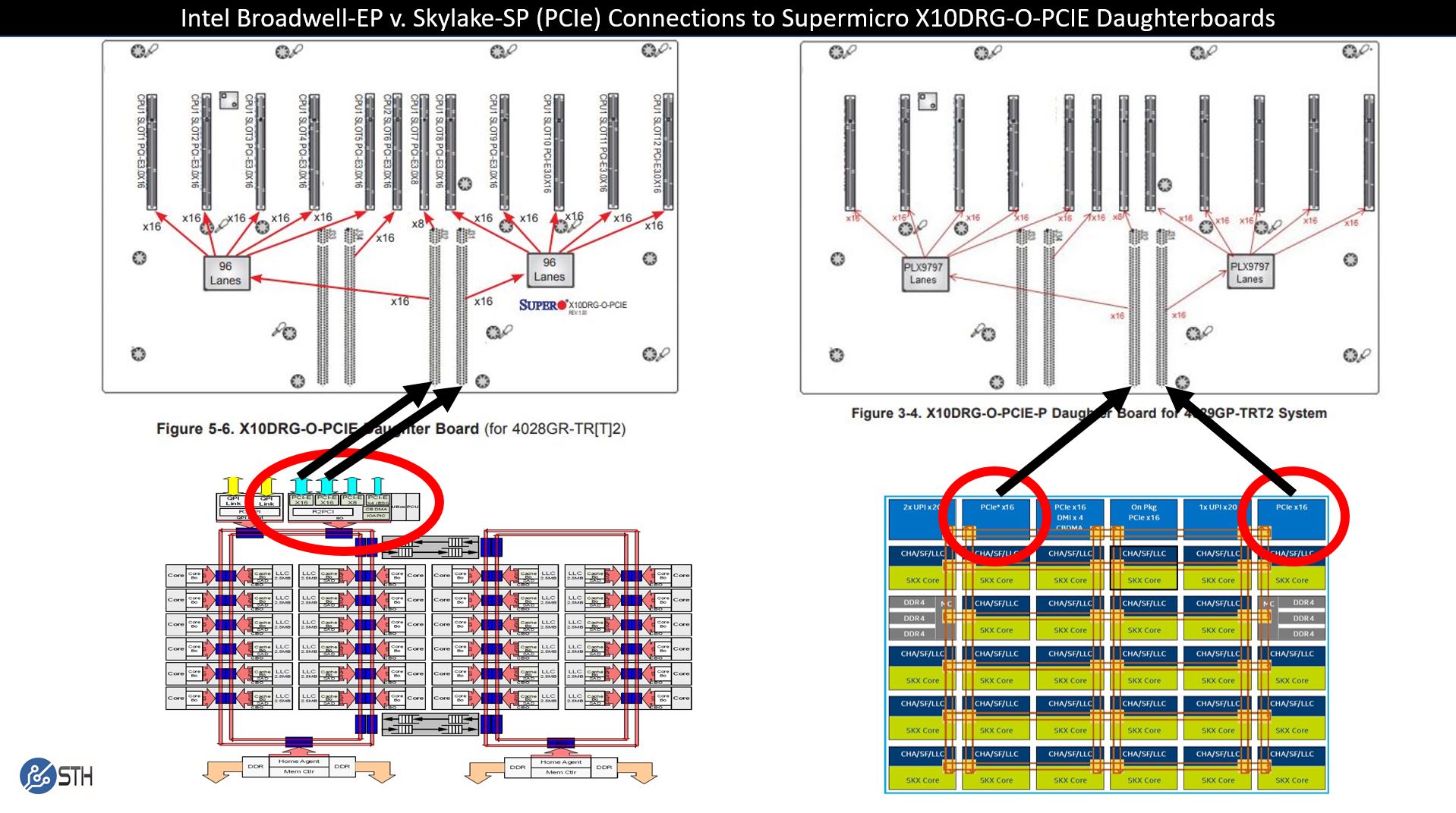
Here we can see how you would connect a 10x GPU daughterboard to a single Intel Xeon CPU to avoid the QPI/ UPI socket to socket interconnect. We circled two PCIe x16 controllers on each CPU diagram. On the Skylake side (left), there is a third available so we picked two, but it can easily be the third.
The implication of this diagram is that the arrows terminate to the same PCIe x16 lanes that feed each of the daughterboards PCIe switches. The arrows originate from two different IIO blocks depending on CPU generation. That difference is the reason that single root 8x and 10x GPU servers are much less common in the Intel Xeon Skylake-SP generation.
One can still make a server that is single root, but it would have a few drawbacks. It would need to have an extra PCIe switch of at least 48 lanes. It would also have a maximum of 16x PCIe 3.0 lanes for all 10 GPUs or a 10:1 oversubscription ratio versus 32x PCIe lanes for a 5:1 ratio today.
Why AMD EPYC Naples Cannot Fill This Gap
For the record, we think that the AMD EPYC “Naples” platform is excellent in many applications, but it is simply not as good for NVIDIA GPU-to-GPU computing. You can read AMD EPYC and Intel Xeon Scalable Architecture Ultimate Deep Dive to get a sense as to the differences of AMD and Intel in this generation.
Understanding the mechanics, we looked back at the materials we had and we could not find the exact view we would want. However, we can make due with what we have. The AMD EPYC “Naples” chips have four dies per package. Each die has on package Infinity Fabric (die to die) I/O. For external I/O there are two 16 lane SERDES links per die that have two primary operating models: socket-to-socket or PCIe.
In a dual socket Naples system, one set is dedicated for die-to-die links across the two sockets. In a single socket AMD EPYC system, one can use all 32 links per die for PCIe. At this point, you may be thinking this is the answer to getting 32 lanes to connect to two PLX switches and 10 GPUs for a single root server. Unfortunately, this is not the case.
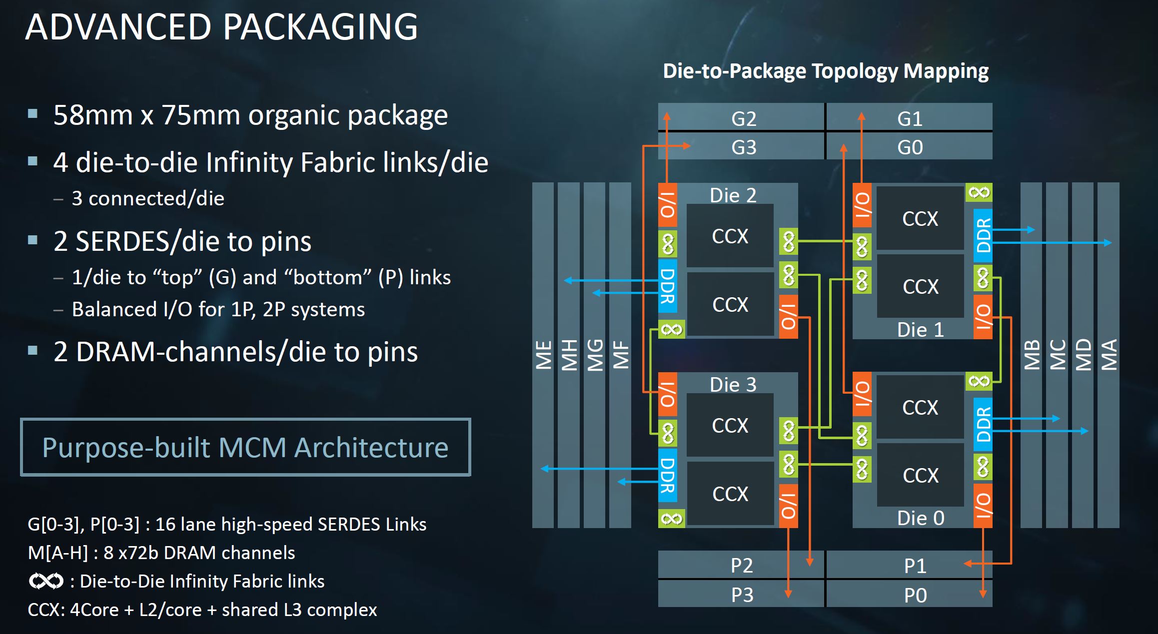
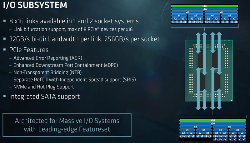
With Infinity Fabric of this generation, each die has both top (G) and bottom (P) 16 lane SERDES links. One swaps from being PCIe to socket-to-socket Infinity Fabric in dual socket configurations. Therefore, there are two different controller locations instead of a monolithic PCIe block as on the Intel Xeon E5-2600 V3/V4 series. One gets back to a Skylake-SP issue of having two PCIe 3.0 x16 controllers on the same die, but not in the same PCIe root.
While one may think that this puts AMD and Intel on equal footing at this point, it does not. The deep learning community does just about anything it can to avoid NUMA transfers. With AMD EPYC, the die that a PCIe switch or PCIe switches connect to only has two DDR4 DRAM channels. Essentially with Naples, building a GPU compute architecture with PCIe switches means that 75% of the systems DDR4 channels are a NUMA hop away. Likewise, although one can get 128 lanes on an AMD EPYC system, that involves connecting the GPUs across NUMA nodes which the deep learning and AI communities avoid if at all possible.
Final Words
The quest for single root is largely driven by NVIDIA’s software considerations. If the companies were perfectly collaborative with Intel not finding NVIDIA as a threat and NVIDIA not trying to push its own margins higher with NVLink for P2P, this may be fixed. There is a chance that tools like nccl could be adapted to work in scenarios with multiple PCIe roots on a single NUMA node/ die making both Intel Xeon Scalable and AMD EPYC more competitive. Business concerns may be influencing the technical requirements here.
With the new Intel Xeon Scalable generation, one can still do single root, but it requires a third PCIe switch and only has a PCIe x16 link back to the CPU through a single IIO module. Likewise, AMD EPYC Naples has a similar constraint. If you want a single root deep learning / AI training server, the Intel Xeon E5-2600 V3/ V4 series platforms are a better bet as they can provide 32 (or technically up to 40) PCIe lanes between the CPU and GPUs in a single root complex.
Stay tuned to STH, DeepLearning12 will be our first 8x GPU NVLink server based on Skylake-SP in what we are going to dub a “DGX-1.5” style system. The final components for DeepLearning12 are arriving the day this article goes live.


 PCIe complexes impacted the ability of the industry to provide single root deep learning and AI servers for the key industry segment)
ASUS has a single root skylake 8 GPU but they’re doing CPU0 > PLX0 > PLX1 so they’re limited to x16 from the diagram like you say https://www.asus.com/us/Commercial-Servers-Workstations/ESC8000-G4/
You’ve got no idea how bad this is for us in the field. It’s ok now since you can still get E5’s but you can’t upgrade to the new gen Xeon Gold and still use P2P.
What this article didn’t talk about enough is that the reason we use single root is to allow inter-GPU traffic. GPU’s talk to each other without having to go back to the CPU.
What is the impact of PLX multi-plexers in the whole system?.
Looking forward to VEGA 20 and NAVI with their own implementation of NVidia’s NVLINK.
What is the impact of 8 vs. 16 PCIe links with current GPU’s like the GTX1080ti (without PLX chips)?
EPYC 2 will support PCIe 4.0 and PCIe 5.0 is on it’s way.
Meanwhile NVidia is laughing it’s but of and people are stupid enough to buy single supply stuff like CUDA, people never learn.
@Lee Chen, thank you. That part was missing for me too, as I had no idea why single root is so important or nice to have.
Hi, very nice work on this artice.
Some other feedback: The “next page” buttons are almost invisible. I saw them only by chance. Consider making them more contrasting.
@Lee Chen
The thing is monolithic architectures are a thing of the past for sever CPUs. The mesh is Intel’s last ditch to keep it alive a litter bit longer but even they will move on to an MCM design sooner than later just like AMD is doing now. If you guys don’t start to adapt your tools to cope with these limitations now, things are just gonna be more painful in a few years. Right now you can still find Broadwell-based CPUs, but you won’t have that option anymore in a few years.
What is the typical CPU utilization of a system like this? Does it even make sense to use Skylake-SP Platinum parts? Does the Xeon D 2xxx have the same issue with PCIe?
This entire discussion is moot because of nvlink. Also what is missing is performance numbers. So what is the effective bandwidth between two gpus on the same plx vs 2 on different plx switches and more importantly the difference in bandwidth between a single root v4 system and the skylake SP one? All the talk means very little without actual performance numbers.
Matt…. you’ve missed the architectural point…. NVLink doesn’t scale using GTX or a large number of RTX GPUs. They’ve got 1080 Ti’s in the top image which don’t use NVLink and are $700 each. If you read their DL10 and DL11 numbers you’ll see, 1080 Ti’s have been the main workhorse of the DL industry since they were released. We use them and all of our competitors use them by the thousands. 2080 Ti’s will replace as prices come down and 1080 Ti’s get harder to source, but it’s a cost thing since you can build 2-3 GTX systems with PCIe instead of 1 Tesla system. V100’s are $9k each which is over a dozen 1080 Ti’s.
We’ve done performance Skylake dual root against E5 single root with 1080 Ti’s at work. Nvidia nccl doesn’t work without single root PCIe on these cards. Skylake’s pcie improvement doesn’t matter here. It varies on model we train, but it’s 20-30% better performance using nccl on E5 single root instead of Skylake dual root.
@Leo Cheng,
@Patrick Kennedy,
Have you checked `nvidia-smi topo -p2p r`, `nvidia-smi topo -m` and the `p2pBandwidthLatencyTest`on a SkyLake like this? (E.g. like Supermicro SYS-4029GR-TRT2?) Is it like this ( https://devtalk.nvidia.com/default/topic/1044817/cuda-setup-and-installation/what-is-the-meaning-of-cns-chipset-not-supported-error-in-nvidia-smi-/post/5301034/#5301034 ) or is it like this ( https://www.servethehome.com/tyan-thunder-hx-ga88-b5631-server-review-4x-gpu-1u/ ) ? Aren’t there any NODE or CNS verdicts?
Supermicro seems to have quietly released a TRT3 variant of the SYS-4029GP, this time with an updated daughterboard (X11DPG-O-PCIE). The manual for the SYS-4029GP-TRT3 has a diagram of the PCIe lanes on page 43, but I’m having some trouble understanding it. By the looks of things, they are using a single x16 PCIe lane from CPU1 feeding a PLX switch that serves 4 PCIe slots at x16, and then another PLX switch in serial that serves 5 more PCIe lanes at x16. From what I gather, that means 9 total GPUs served by a single PCIe root on CPU1. Supermicro still doesn’t advertise single root complex or RDMA support, but is this their answer to that problem? Are they not advertising single root complex because the remaining PCIe slots are not actually on a single root? Any idea how those 5 PCIe lanes hanging off another PLX switch would perform vs the the older daughterboard?
As of September 2019, Supermicro now advertizes both SYS-4029GP-TRT2 and SYS-4029GP-TRT3 as single root complex:
TRT2: “Single Root System for excellent GPU peer to peer communication with sufficient CPU to GPU throughput”
TRT3: “Single Root System, Cascade Mode for maximum GPU peer to peer communication”
“Cascade mode” probably refers to the serial connection through the 2 PLX switches. As for TRT2, it’s unclear to me why they’d advertise it as single root.
Anyhow, does anyone have a performance comparison between single root E5 and Cascade Lake builds on these boards?
The E5 would have to be on a SYS-4028GR-TR2, as the 4029GP systems do not support E5.
The GPUs for the comparison would also ideally be Quadro RTX 6000 or Titan Xp. I just found out that the GeForce cards from the Turing generation (Titan RTX, RTX 2080 Ti…) cannot do P2P at all, so there’s no reason not to use the latest generation of CPUs with them.
Does anyone know if the PCIE backplane is a completely passive device or if it is tightly coupled with the motherboard/motherboard bios?
Could I run the PCIE connector through a ribbon cable back to another mobo with a single epyc 7002 series for example?
I want to set up a machine for LLMs and need a lot of ram since I can’t afford more than ~128GB in VRAM.
I’d like to have all the ram in the system on the same cpu so no intersocket voodoo is occurring and slowing it down.
I really like these PCIE switches for my use case since If I can put a superfast SSD array for temporary storing the model on the GPU side of the switches so I don’t have to traverse the CPU for PCIE access and would be able to do something like mmap the VRAM directly to the SSD array on the fast side of the switch.
This obviously is not as fast as ram but I would have thought the extra cpu cycles I get to skip by bypassing the cpu would make up for it especially if I built the storage array with optane (Expensive but definitely more affordable than a single high vram GPU)
Comments are closed.