
This week I was filming some content for YouTube with Supermicro in Santa Clara at an undisclosed location. As part of the project that folks will see next month, we had a NVIDIA BlueField-3 DPU on hand. I saw one at SC22, but I was told that was a Lenovo model. It turns out, that was incorrect. This sample was being used at Supermicro and it looks similar.
NVIDIA BlueField-3 400Gbps DPU Exposed
We originally took photos with this atop a 400Gbps ConnectX-7, NVIDIA H100 PCIe, and some Intel Data Center GPU Max 1100 series GPUs, but we realized that the Supermicro server all of those were in is not yet released. Luckily, we took backup photos on a white background.
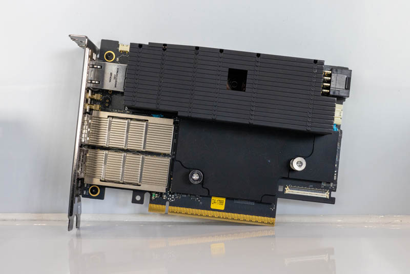
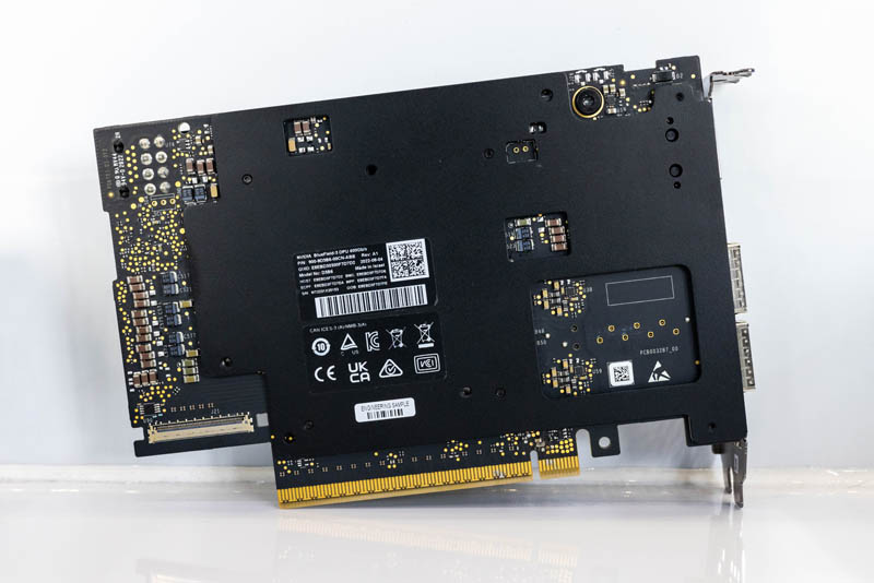
Here we can see the same heatsink design that is offset from the optical cages to provide more airflow to high-speed optics. We also see that BlueField-3 is becoming a double-width model.
We have an 8-pin power connector here, so we expect this is a higher-performance model. This is also the second BlueField-3 with the blue glue. We are not sure if that color is a coincidence, but we hope it is not.
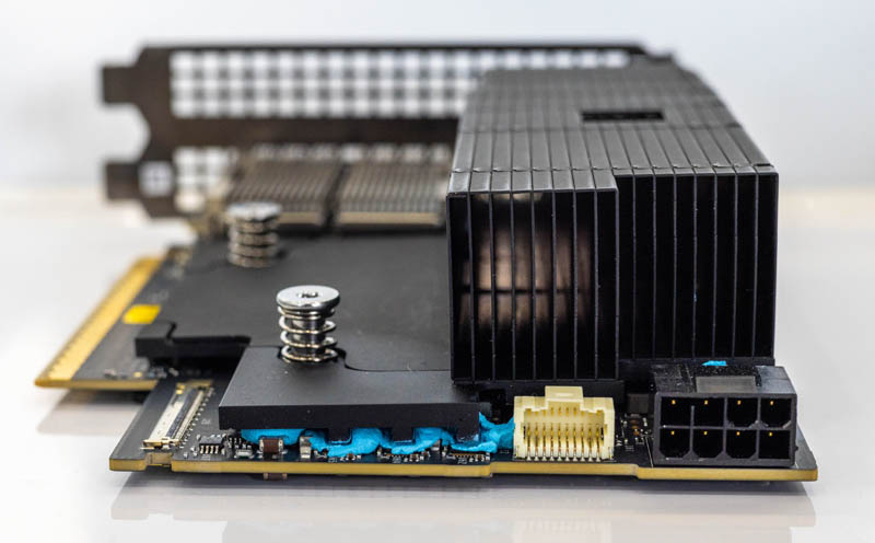
There is a lot of blue paste/ glue. These BlueField-3 cards are about as rare as Sumatran Tigers in the wild. We have still not been able to get one. As a result, we did not get to take the heatsink off.
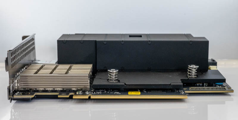
These cards now have a nice backplate.w
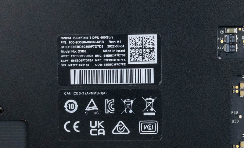
We can see that this particular model was only produced in August 2022 and carries a D3B6 model. There is not a lot on the NVIDIA 900-9D3B6 out there.
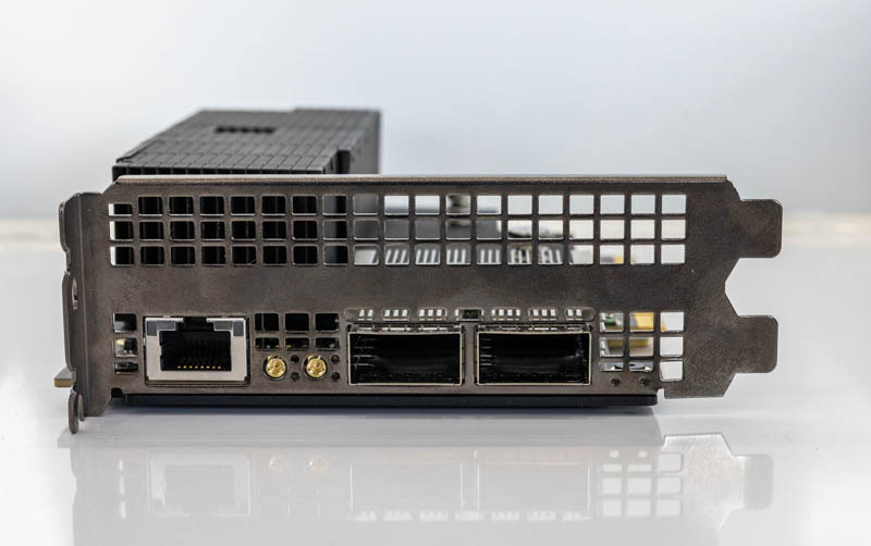
Still, we can see a management port, time sync ports, then two 200GbE ports for a total of 400Gb/s.
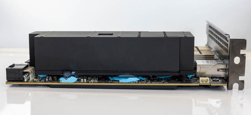
Still, it feels like this is a significantly higher-power solution compared to the BlueField-2 DPUs that were single-slot solutions.
Final Words
This week between the Marvell analyst event and preparing content for January 2023 launches, we were quite busy. A lot of the hardware we cannot show until next year, but this is one where it is a shipping product so we can show it. We just hope that NVIDIA releases more information on these beyond that they are 16 core Arm A78 PCIe Gen5 cards, with an onboard BMC and 16GB of onboard DDR5.
Unfortunately, this was not a case where I was able to take the DPU back with me to Austin.


The offset heatsink also looks like it could allow for a half height PCIe cards/ or PCIe extender/risers type thing to fit if needed. For cases when there is another PCIe slot present right below the one x16 slot for the DPU.
It’s kinda a weird case – it looks like NVIDIA needed a full width PCIe slot to fit the IO but a 1 slot cooler eyeballing would have been pushing colling wise for servers without a relatively high airflow with proper ducting. As more stuff goes water cooling and the fan watt budget settles down this could come into play more often.
The time sync ports are very interesting. Not sure I’ve noticed those before on other NICs/DPUs.
Could you maybe do an explainer on that infrastructure, what it looks like, etc?
The two time sync ports (1PPS and 10Mhz) are standard on high-end electronic trading and capture cards. The PPS port very accurately signals when the second starts, and the 10Mhz is what second it is. Both are then used to set the clock for the BF3 chip so that as it timestamps packets, those timestamps can be within a few nanoseconds of real-time.
The Heatsink is shaped that way to ensure that the two 200Gbps QSFP sockets receive cool air as they can each draw some serious power as well, as they may need to support active optical cables. If I were to guess, this is a vapor chamber heatsink, and it’s migrating all the heat off the BF3 chip and pulling it toward the top of the card.
Oh, and the blue goo is very likely a heat-conductive silicon-like compound used to wick all the heat off various components and transfer it to the heatsink.
The backplate is also provided to give the card more rigidity and the fasteners for the heatsink end up screwing into this plate so the PCB is sandwiched between the two, and then the normal mechanic stresses are then shared between the heatsink and the back plate rather than all carried on the PCB.
Comments are closed.