
A cool feature of Hot Chips 34 is that we again get to look at some chips that we would normally not get to see (unless we bought and somehow imported them.) One of those in HC34 is the Biren BR100. The BR100 is a GPU designed for GPU compute in a data center and uses a number of advanced features that make the design very interesting.
Note: We are doing this piece live at HC34 during the presentation so please excuse typos.
Biren BR100 GPU for Datacenter Compute and AI Workloads
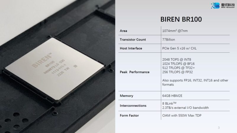
This is certainly something different. The BR100 is a 77B transistor 7nm chip. Many of the next-gen GPU are going below 7nm, so this is a big chip at 1074mm2. It sounded like the company said that the compute tile is 477mm2. The NVIDIA H100 is a 80B transistor chip. One other interesting aspect is that this is a 64GB HBM2E part. That is going to be lower than the Ponte Vecchio, H100, and also the AMD MI250X. It is more like half of the MI250X memory. This is likely done to lower cost. At the same time, we should be comparing this to the H100 and Ponte Vecchio as it is a PCIe Gen5 GPU with CXL.
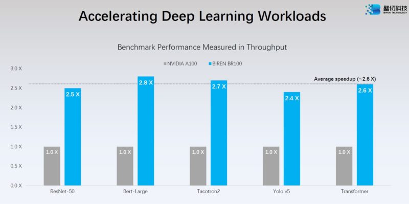
Just for some reference, the Intel Ponte Vecchio at 1.6GHz was just disclosed at 839TFLOPS for XMX BF16 but that may or may not be the operating frequency when that ships. Biren says its chip is much faster than the NVIDIA A100 in deep learning.
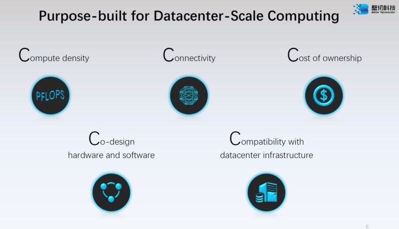
Here are the five C’s on Biren’s focus. Cost is always a big deal when companies look to compete with NVIDIA.
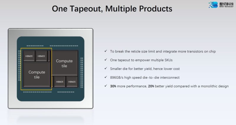
Here is how Biren is making its chiplet-based GPU. We can see two GPU compute tiles. There are then two HBM2E packages. The 896GB/s die-to-die interconnect is more than 2x the die-to-die interconnect on the MI250X.
Biren has its BR100 for its OAM platform and the BR104 for PCIe. Since it uses chiplets and is modular, there is a BR104 without having to re-tape out a new design. To us, the Biren Hearten server is very interesting.
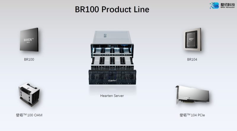
Folks are going to wonder what the Hearten Server is. Since the BR100 GPUs are OAM, and we see eight of them with external connectivity, it is likely that they are using the OCP OAM Universal Baseboard or UBB. This is now OAI.
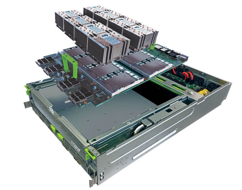
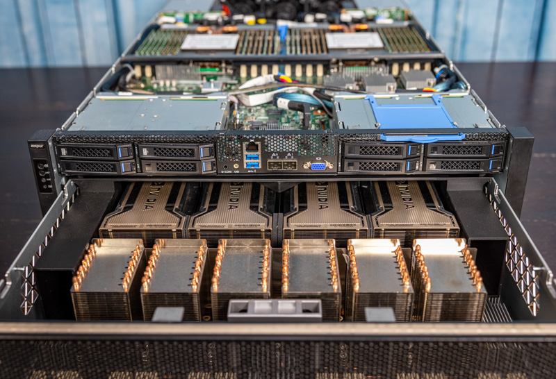
The server itself looks like a variation of the Inspur accelerator platform, but with a UBB tray instead of a NVIDIA A100 tray. You can see the top section from our Inspur NF5488A5 8x NVIDIA A100 HGX and Inspur NF5488M5 8x NVIDIA V100 reviews (video here.) Our best sense is that it is a version of these platforms but with the OCP OAM UBB inside.
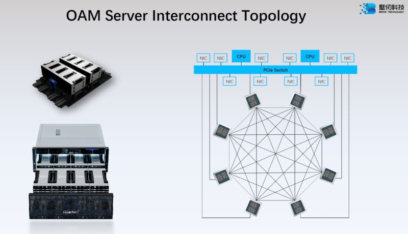
OAM is designed to have multiple connections. BLink is Biren’s interconnect between GPUs.
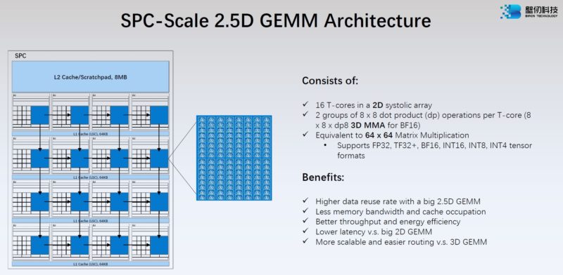
Biren has a Streaming Processing Center with 8MB of L2 cache plus the compute resources. In this diagram, also important is that the GPU has video encoders and decoders. That is a big deal for AI since so much is based on processing video.
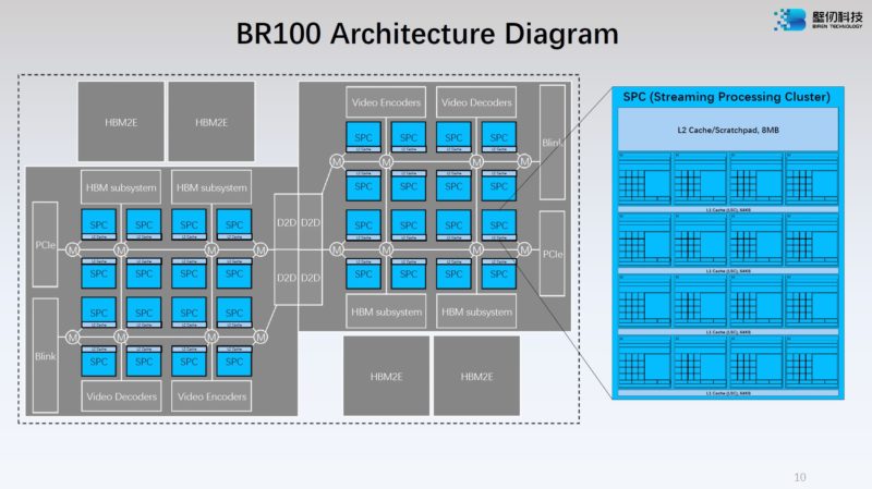
Each GPU compute tile has 16x SPCs. Each SPC has 8MB of L2 so there is 128MB on each tile and 256MB on the Biren GPU.
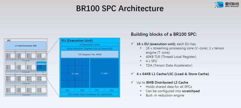
Each SPC also has 16 EUs.
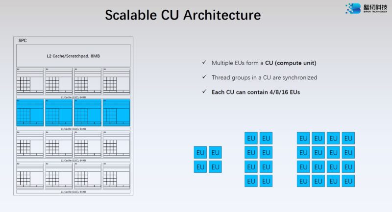
Biren designed a SIMT GPU for general-purpose compute. With the BR100, the compute unit or CU, can be split into 4, 8, or 16 EU chunks.
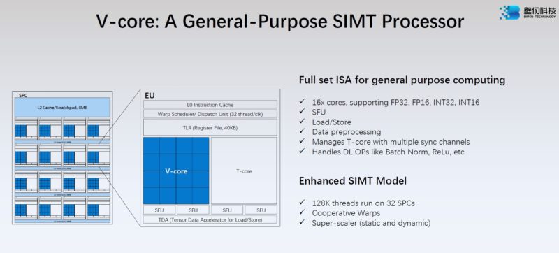
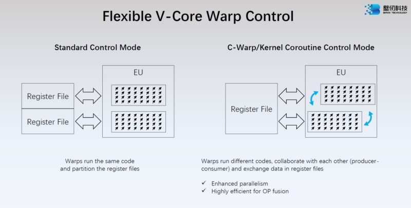
Here is Biren’s detail on the V-Core Warp Control.
The T-core seems to be Biren’s tensor core that deals with matrix math.
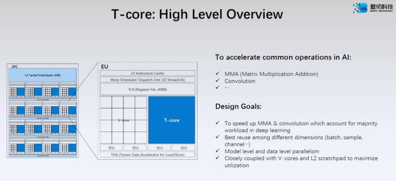
Here are the specs on the T-core and is how Biren is hitting the previously mentioned performance figures.
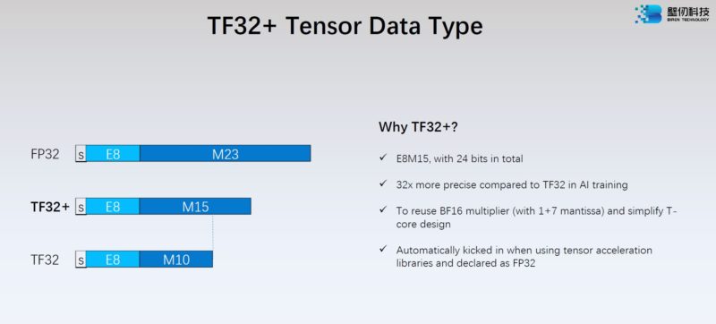
Biren has its new data type TF32+. This is between TF32 and FP32.
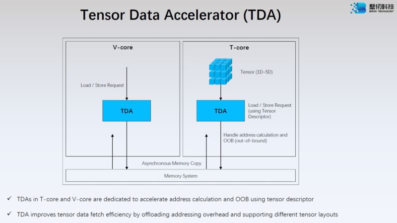
Biren also has the Tensor Data Accelerator or TDA. NVIDIA just discussed its asynchronous data mover, the TMA, at Hot Chips 34 as well.
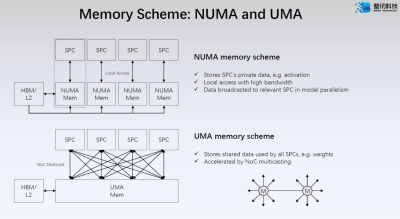
Here is Biren’s memory scheme of NUMA and UMA depending on where the data sits.
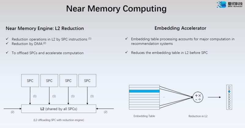
Biren has a Near Memory Engine to make L2 cache use more efficient.
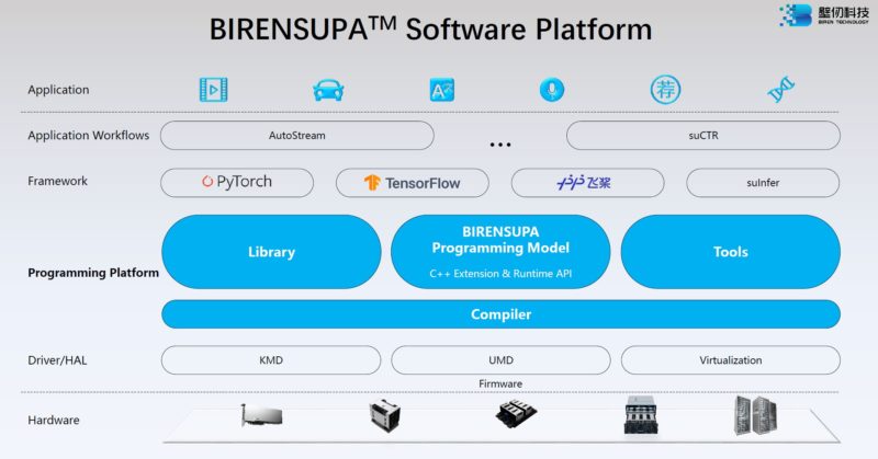
Along with building a GPU in three years, Biren also has its middleware software platform.
Here is the company’s summary slide.
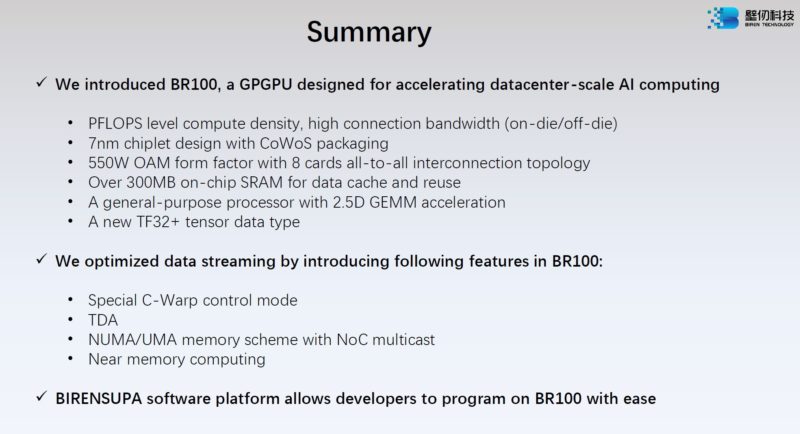
There is a lot of really interesting technology here.
Final Words
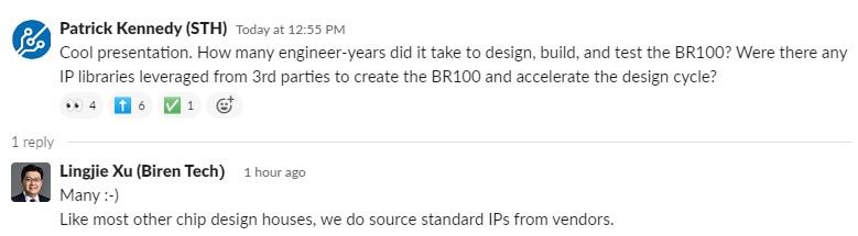
This is a cool-looking chip. At the same time, perhaps the most amazing aspect is that Biren was able to create the BR in less than three years. The company said that it started with targets in 2019. In under three years, they made a multi-tile GPU, with all of the ancillary features. That is an amazing engineering effort when you compare it to established players like NVIDIA, AMD, and Intel and their large engineering teams.
I asked the company how many engineering years it took to make the BR100 and if they are using external IP. This is the reply I received from the company’s co-founder Lingjie Xu who co-presented the talk.
The company said that it has already submitted MLPerf Inference performance numbers, and we should see the results in a few weeks. The company also said it is waiting for Intel Xeon Sapphire Rapids for CXL compatibility testing but it believes its part is ready.


So what does the G in GPU stand for in this particular chip?
@Patrick, do you anticipate that at some point we’ll be able to buy/import these chips to Europe/USA?
Most likely yes. The challenge is now that the US restricted A100 and H100 along with MI250 sales to China, it is reasonable to expect China to restrict exports. The other challenge is that now this becomes a more prominent architecture within China and that is bad for NVIDIA/ AMD.
Comments are closed.