
At Hot Chips 34, Lightmatter is making a splash. Its new product, the Lightmatter Passage is a photonic wafer-scale interconnect that ties chiplet processors with silicon photonics and co-packaged optics to create something huge. This is a very cool presentation. It comes from Lightmatter that we have covered a few years ago. Two years ago we covered Lightmatter Mars SoC AI Inference Using Light at HC32.
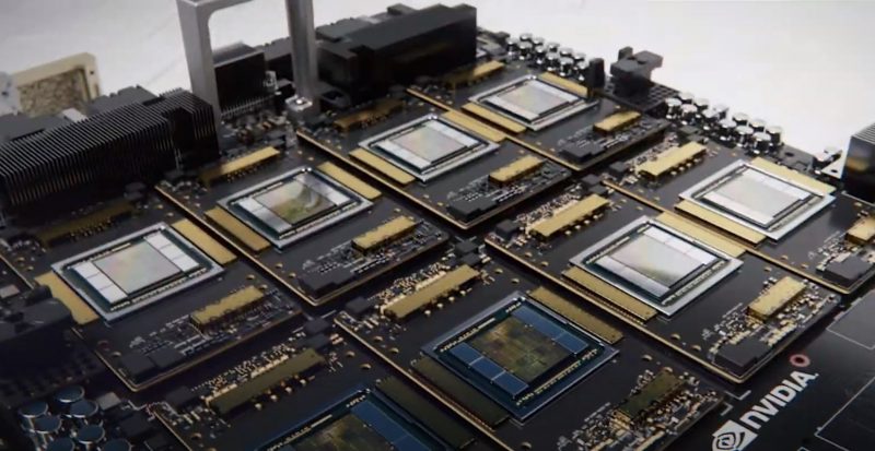
To make it a bit clearer about what is being shown, think of Lightmatter Passage as a base layer. In that base layer there are lasers to generate light, optical pathways and switching/ routing capabilities to move data and provide connectivity. On top, there are places to put chiplets that can be compute, memory, or other accelerators/ devices. The placed chiplets can get their interconnect to other chips through the Lightmatter Passage base layer. That Passage product then has optical links externally for building larger systems. In other words, imagine instead of using an electrical/ PCB solution like we see on this HGX A100, imagine if it was optical, and the NVSwitches were built into the optical pathways.
This is a bit abstract, and that is not a perfect analogy, but the Lightmatter folks tried explaining the background from an optical networking side, rather than looking at something in-use today. That is probably the closest I could think of quickly to show you.
Note: We are doing this piece live at HC34 during the presentation so please excuse typos.
Lightmatter Passage Photonic Wafer-scale Interconnect
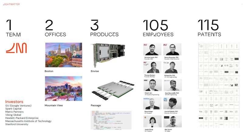
Lightmatter is a 105-person company based in Mountain View, California (where STH was before moving to Austin last year.)
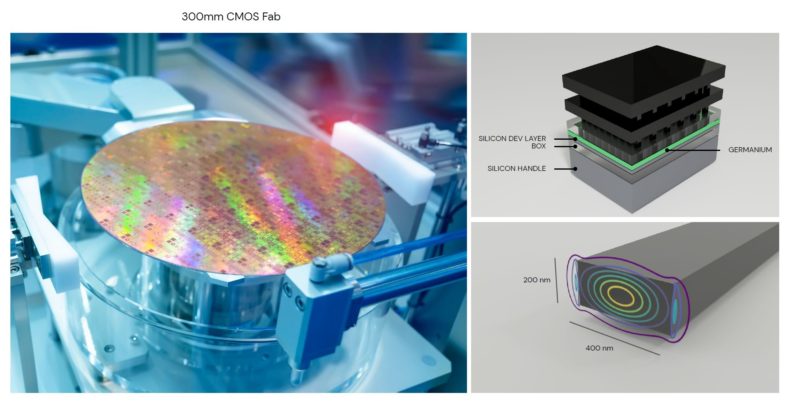
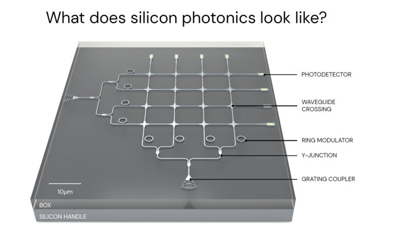
Silicon photonics today is generally made on 300mm CMOS with different layers.
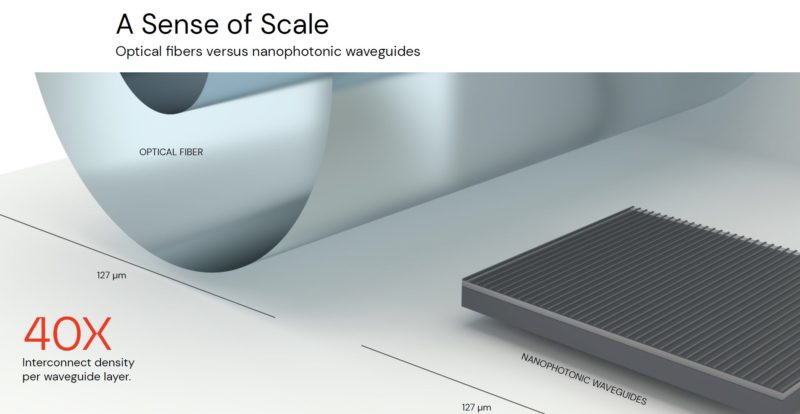
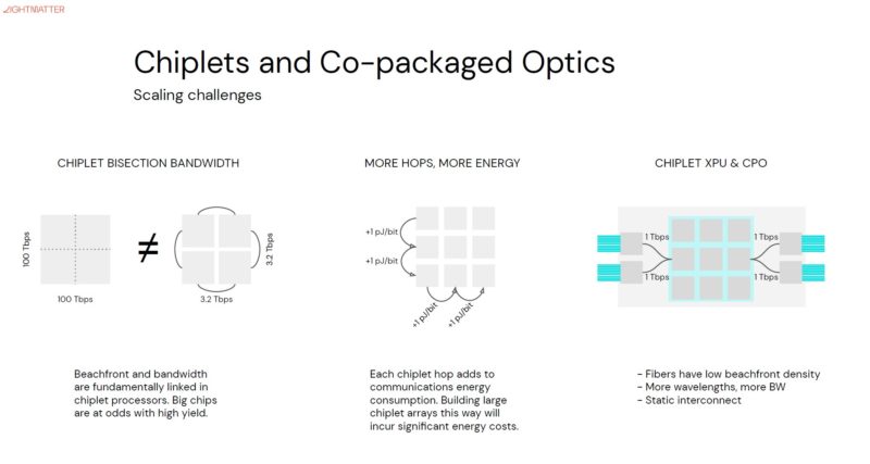
There is about a 40x interconnect density per waveguide for nanophotonic waveguides versus optical fiber. Simply fitting optical pathways into a form factor that works with the density and size requirements of data center chips is a challenge.
This is a photonic circuit. We are not going to go deeply into this one, so if you want to learn more, there is always search.
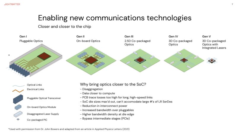
These are the generations of optics moving closer to chips. We have looked at co-packaged optics before, but going beyond pluggables will be important. Eventually, having co-packaged optics with integrated lasers is the goal.
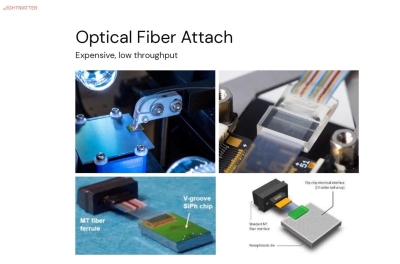
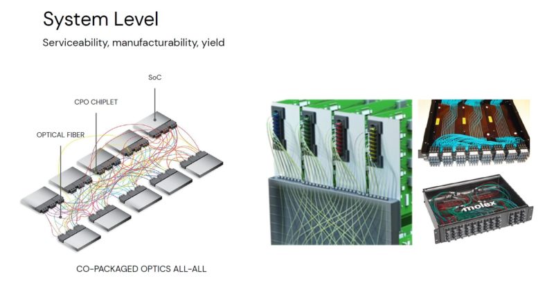
These are photos of the manufacturing process for optical fiber attach. This is the approach Lightmatter says will not scale for chiplet architectures.
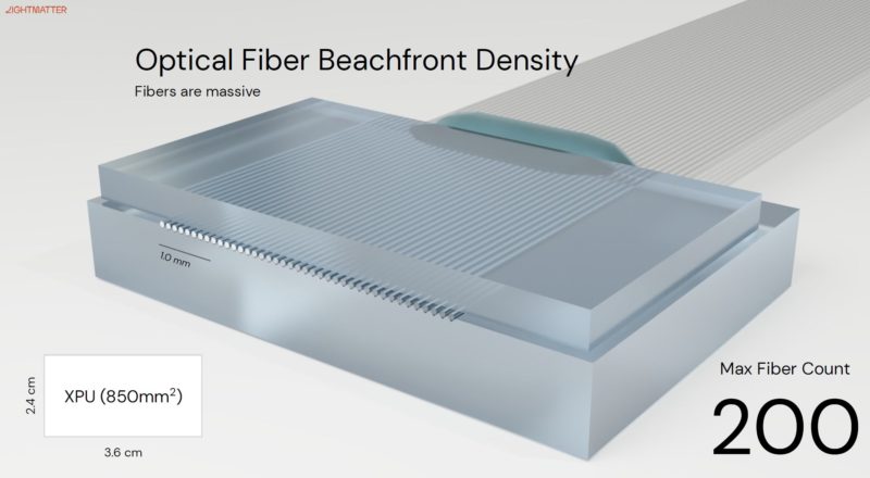
The maximum density one can get in 3.6cm is roughly 200 fibers. This is a challenge for the chiplet era and is a function of how large fibers are.
One of the big challenges with the industry now is that having electrically connected chiplets adds more power consumption and bandwidth/ latency challenges.
On the left, there are ten chips, and each of these have all-to-all connectivity. One can use a fiber loom, but it is not serviceable, or at least easily serviceable.
This is Lightmatter Passage that seeks to shake up this model.
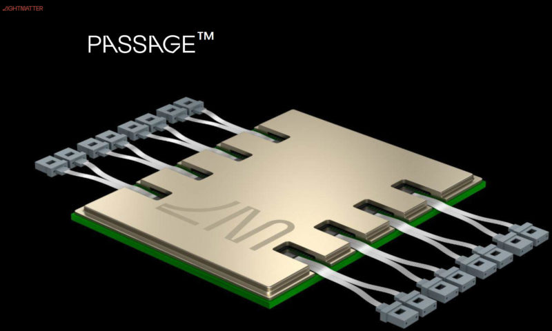
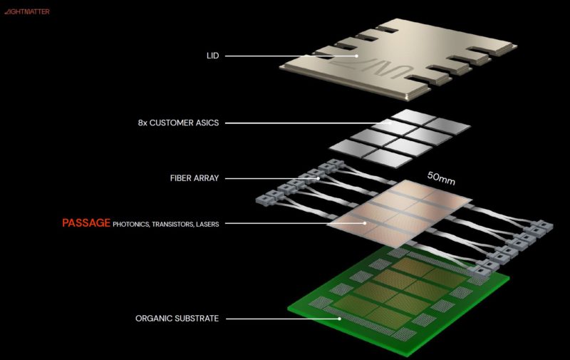
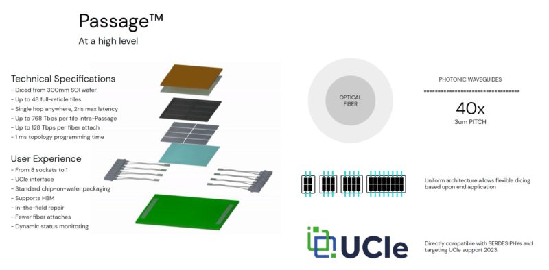
There are eight ASICs on tiles. Each ASIC goes to the Passage Silicon photonics wafer. Passage has its own optical fiber array.
Passage is 2×4 or 6×8 right now, but it is configurable in size. Each Passage tile can connect all of the ASICs directly.
Integration with Passage uses TSV’s for power and signaling to the array chips on top of Passage. The silicon photonics/ and optics run through the package. Typically the entire package is liquid cooled.
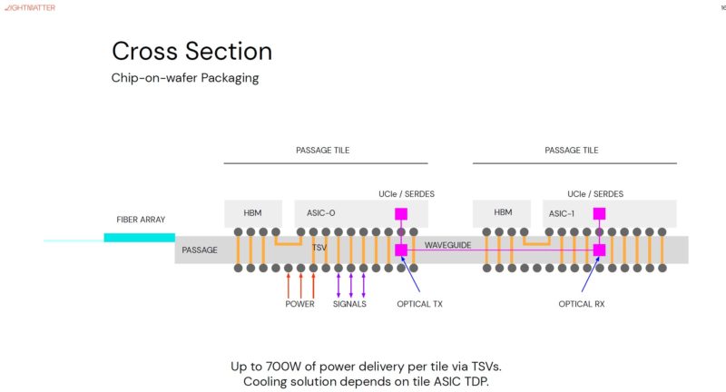
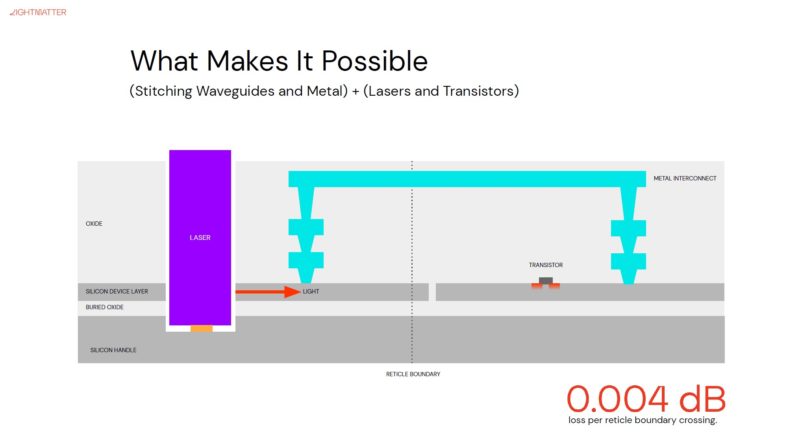
Passage has integrated lasers and transistors, along with the waveguides and metal. Effectively, this is the interconnect between different ASICs in a system.
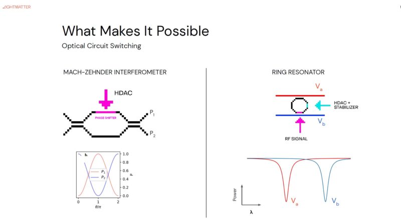
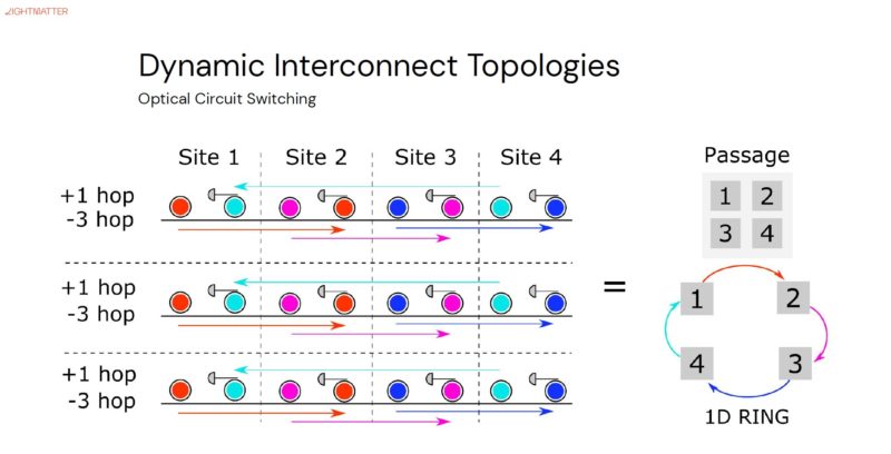
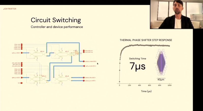
Lightmatter uses optical circuit switching to guide light and different wavelengths. This allows for routing using light.
This is what the optical switching looks like. This video was posted in 2017, and has 72 views as of posting this.
Having the ability to do this switching and routing, Lightmatter can use wavelengths and change interconnect
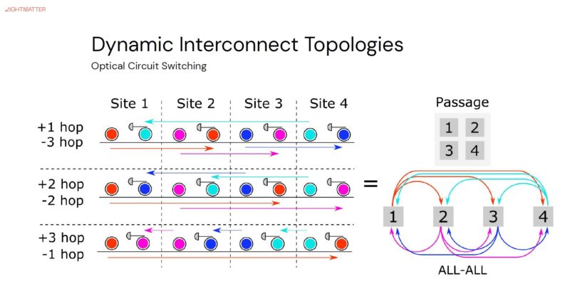
Lightmatter can reconfigure the entire interconnect in under 1ms. In this example going from all-to-all to a 1D ring topology.
This is a 300mm wafer in a 6×8 grid. The center shows a chip socket on Passage.
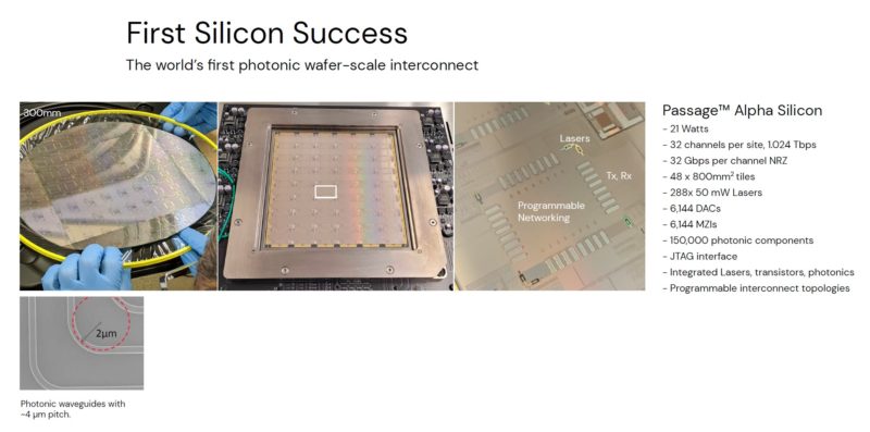
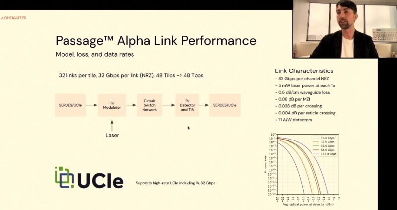
Lightmatter says it can handle the high-speed UCIe 32Gbps spec speeds for chiplet interconnects. Direct SerDes the company thinks it can hit 112G speeds.
Here is a slide on the company’s circuit switching.
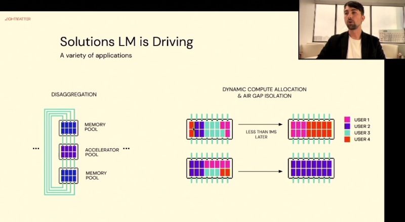
Here is a really interesting use case. Building a chip on Passage allows a cloud provider, to provision more memory or compute resources dynamically. When it is time for reconfiguration that can happen quickly. Instead of using provisioning on a die, CPU, GPU, accelerator, or another package, one can provision “air gapped” dies or memory using the switching fabric.
This is extremely cool!
Final Words
Co-packaged optics and silicon photonics are still a few years from being mainstream integrated on chips. The advantage is simple though. With optical communication, bridging longer distances can be done less expensively and at lower power. With Lightmatter’s switching technology not only can it simplify cabling, but it also allows for chips to span larger topologies than are realistic with purely electrical approaches. We discussed Intel “Lightbender” in Raja’s Chip Notes Lay Out Intel’s Path to Zettascale. Imagine being able to take all of the HBM chiplets on the GPUs we showed earlier today and placing them off-chip for greater capacity. Lightmatter Passage does this at a larger chip scale.
Co-packaged optics is coming to networking. Broadcom’s new Tomahawk 5 has it as an option and we saw it in an Intel lab in 2020.
Overall, this might be my favorite presentation I saw on the HC34 agenda. This is really innovative technology that could be disruptive.


Wasn’t your father a bigwig in the optical networking space?
Anil – He is retired and has been out of this for some time. We started covering networking more when he retired to avoid conflicts.
This article in its entirety is even better than its subject. Good luck to a Big Four compared to this piece.
Looks like a nice method.
Not sure why people are wasting their time on things like this when POET Technologies has the technology to change the way we think about optical semiconductiors.
After watching the video.. what Intel has done, is very impressive.. the future of optical chips is looking very bright!
I wonder how what POET is coming out with compares to what Intel has here.
very cool
Curious to hear if anyone with the technical knowledge reading this article could comment on how this compares with POET’s Optical Interposer?
Comments are closed.