
When Intel released a few teaser images and a presentation that was originally supposed to be shown at OFC 2020 before current events canceled most shows. In that presentation was the company’s work on advancing co-packaged optics. I immediately sent a note to Intel and asked if the demo was down the street in Santa Clara, California. Since it was, I was able to go and check it out in person and tell you about it instead of just re-posting Intel’s slides.
Intel Co-Packaged Optics with Silicon Photonics Video
This year we are producing more content both in written format as well as with video. If you prefer to listen along you can check out the video version.
That video has a few more angles of the switches that we are talking about in this article as well if you see something and may want a different angle.
Why We Will Have Co-Packaged Optics
The short answer here is that companies that use a lot of switches such as Facebook are driving this change. Hyper-scale companies deploy tens of thousands of switches in each significant data center and therefore deploy millions of optical transceivers. These same companies are also pushing for faster networking to handle internal traffic to the point that 100GbE is common and we are driving to 400GbE and then 800GbE speeds very quickly. As we move to those higher-speed links, current pluggable optic technology no longer scales. We covered this during the 2018 OCP Summit, where Facebook was pushing for co-packaged optics in the 400GbE generation.
Setting the stage as to why the industry is pushing in this direction, let us start from the most basic question: what is a pluggable optic. For years, networking gear has used optical modules that convert electricity to light so that the electrical systems in devices such as servers and switches can efficiently travel distances over light. There have been many pluggable form factors over the years, but some common ones are SFP+ and QSFP+ for the 10/40GbE generation and now SFP28/ QSFP28 for the 25/ 100GbE generation.
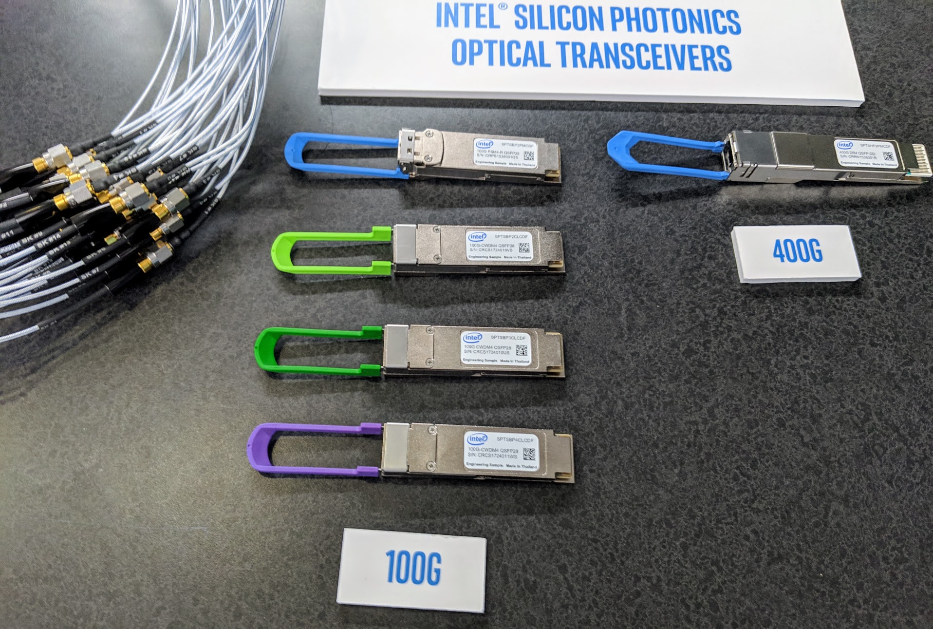
By standardizing on form factors, volume manufacturing can drive prices down. Equipment vendors can design to the common modules and module vendors can innovate, bringing in market competition. It was not long ago that a 100Gb long-range optical module was well over $10,000 and now one can buy those modules for less than 1/10th that price.
Another benefit of pluggable modules is simply their modularity. For example, one can use copper DACs for in-rack server-to-switch communication, short-range optics to reach the end of a row of racks in a data center, and long-range optics to go 10km or 40km to a different data center. With standardization, one can mix-and-match these capabilities in a switch and optimize on requirements and TCO. Modularity also means switches are produced with cages for standardized transceivers and then tailored for a specific deployment as a final step, often at the data center.
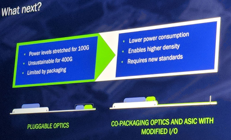
After decades of pluggable optics, as one might imagine we are now seeing constraints to this ultra-flexible solution.
The modules themselves have to receive an electrical current. They then need to convert that current to optical signaling through integrated lasers and ensure that signaling is a high-enough quality to meet specifications. These same modules also need to do the opposite and receive photonic signals and convert that signaling to electricity.
On the electrical end of the module, one then needs to drive electrical signaling to and from the module. For example in a switch, that electrical signaling has to go from the switch chip to the optical module. While the data is moving to and from components, one needs to ensure that the transmission is happening accurately. That means some signal processing needs to happen at either end of the link and the requirements of that signal processing go up the less accurate of a link. That is why we see inexpensive 25GbE optics and NICs but 25Gbase-T is not feasible for the time being. Copper cabling has a lower signal to noise ratio than fiber so the processing is too great at 25GbE.
In the 1Gb generation, this was not a significant issue inside switches and servers. Modern PCB can transport 1Gbps of data efficiently. The signal processing that is required to ensure a 1Gbps transmission is transmitted accurately is not burdensome. At 100Gbps, we see transmission through PCB use a lot of power, on the order of tens of percent of total switch power. Beyond energy, other signaling components required.
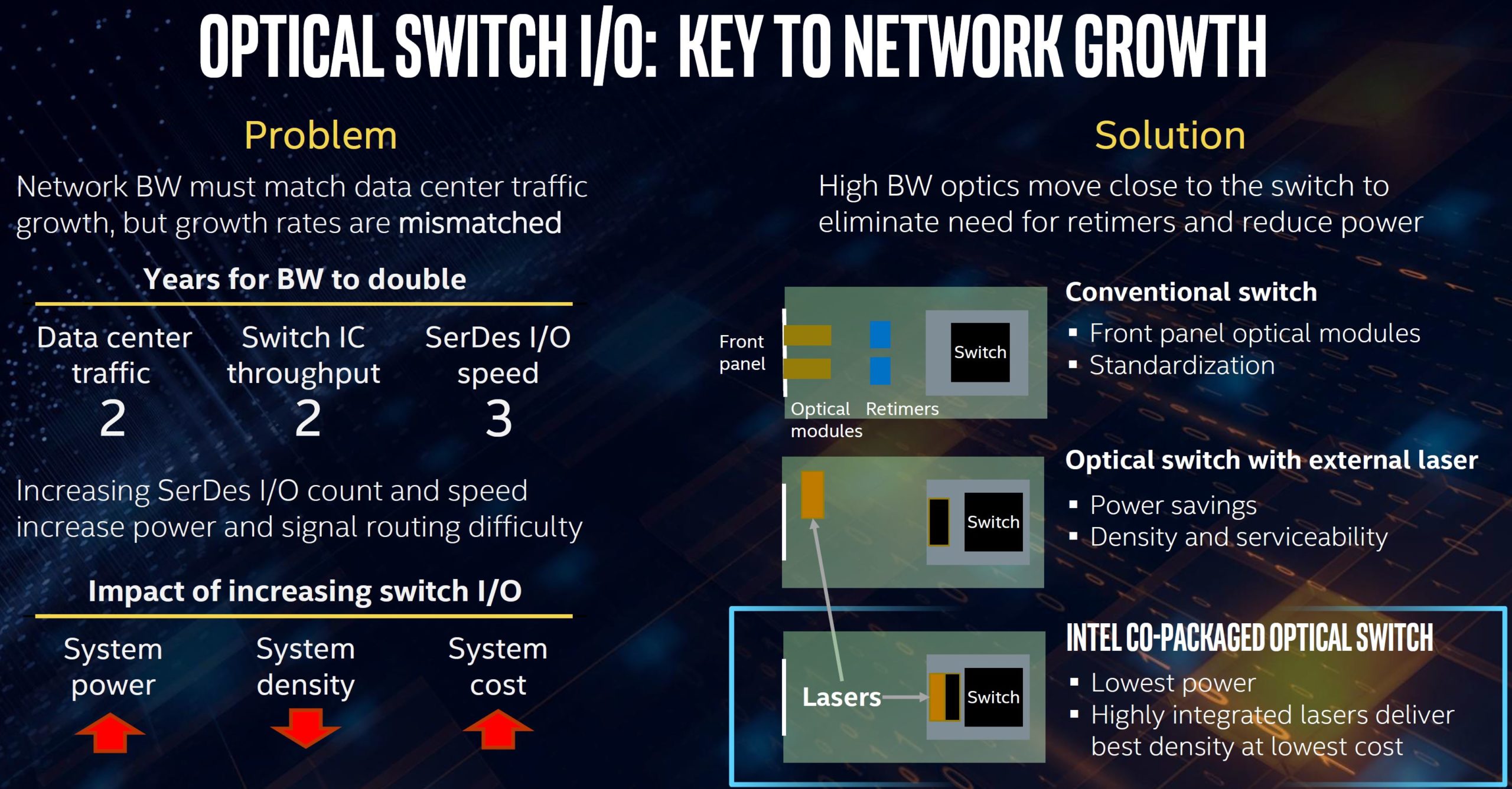
Looking ahead, to 400GbE and 800GbE generations this will go from burdensome to prohibitive.
Another aspect is density. On a 1U switch, one can only place somewhere around 32 to 36 QSFP28 size ports. There is simply only so much area one has on a 1U faceplate. Each module with all of the components to drive transmission and conversion also needs its own metal casing, insertion and removal mechanicals, and so on. Even with a full 32 to 36 ports, if you look at the size of the fiber connector compared to the size of a QSFP28 module, you will immediately see that the module takes up significantly more faceplate area. That has a side-effect of reducing airflow through the chassis which is a particular challenge with dense solutions such as switches.
Summing that up, we now have challenges with the complexity, size, power consumption, and thermals pushing electric signaling to optical networking modules. Those are a lot of challenges in order to maintain ultimate flexibility.
The Next-Gen Intel Silicon Photonics Co-Packaging Solution
When Intel purchased Barefoot Networks for its programmable Ethernet switch silicon it was clearly done with this co-packaging in mind. Indeed, STH even had a picture from that 2018 OCP Summit Facebook keynote in our piece covering that deal. The clear move was to integrate the high-momentum silicon photonics networking side with switch silicon as Intel looks to expand data center silicon TAM.
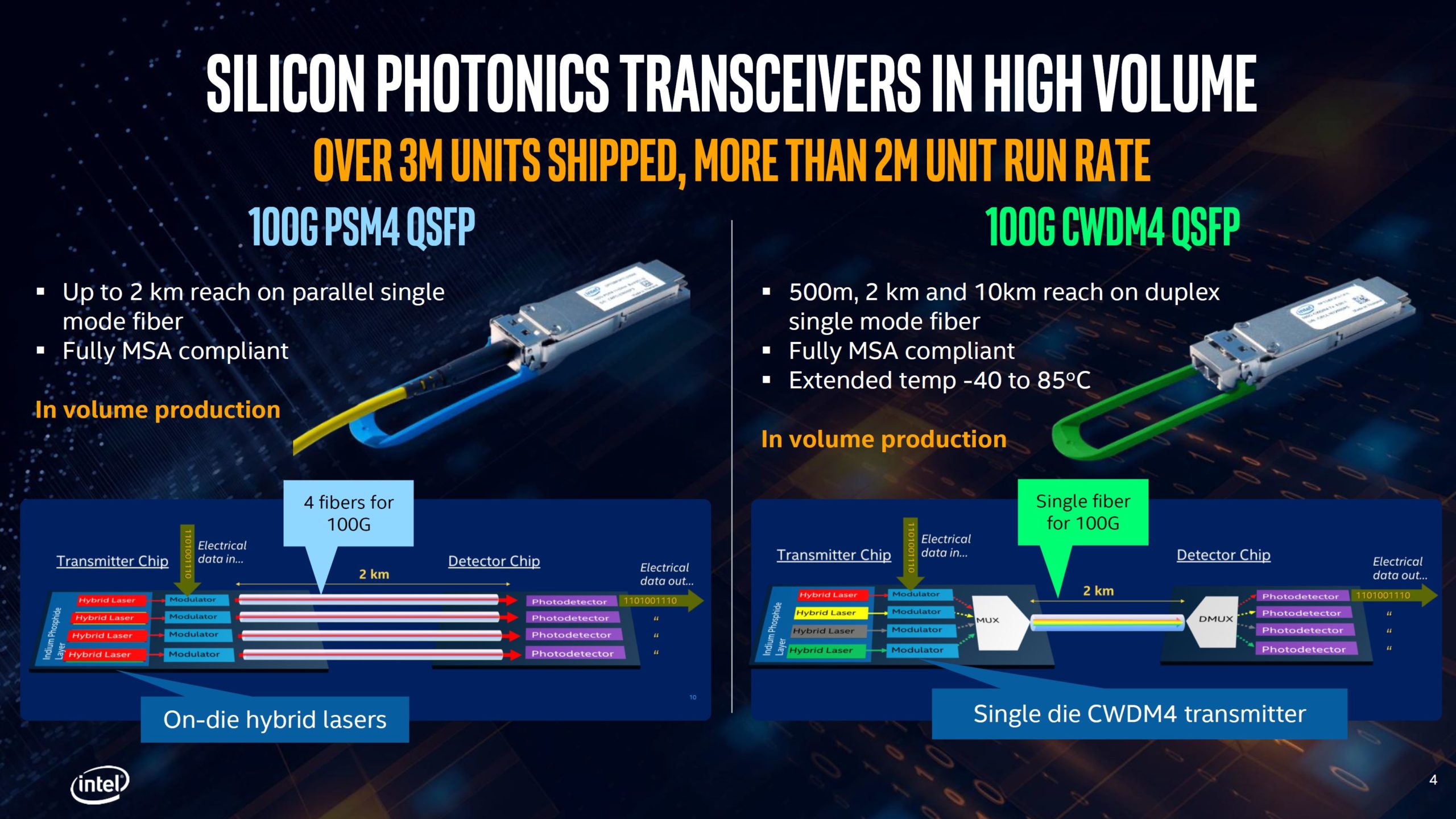
For some sense of Intel’s Silicon Photonics momentum, we attended Intel Silicon Photonics Update at Interconnect Day 2019 where Intel said it shipped a million modules. Today, it has shipped over 3 million modules. A key reason for that success is the integration leading to orders of magnitude better reliability in the field.
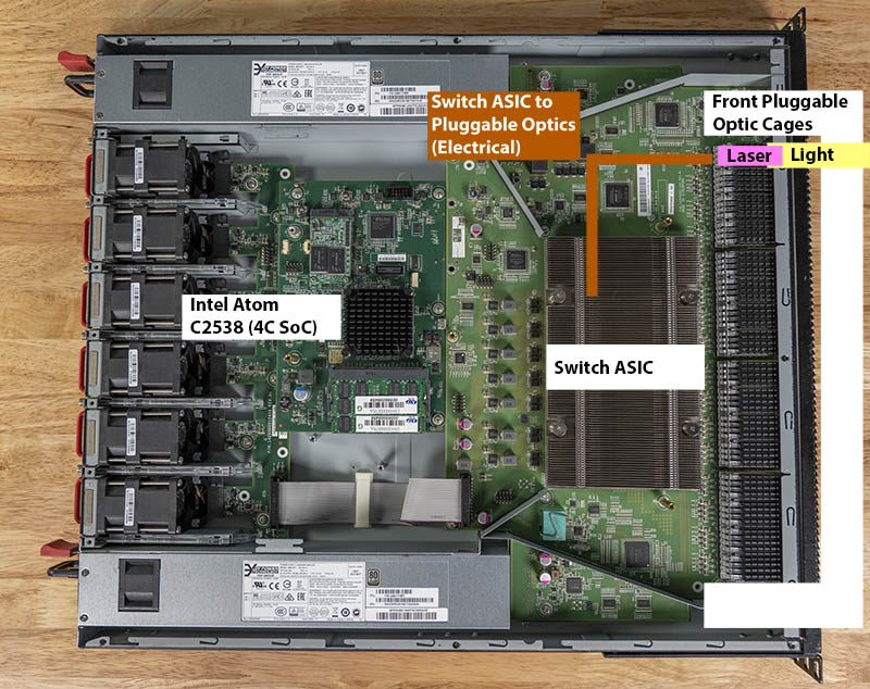
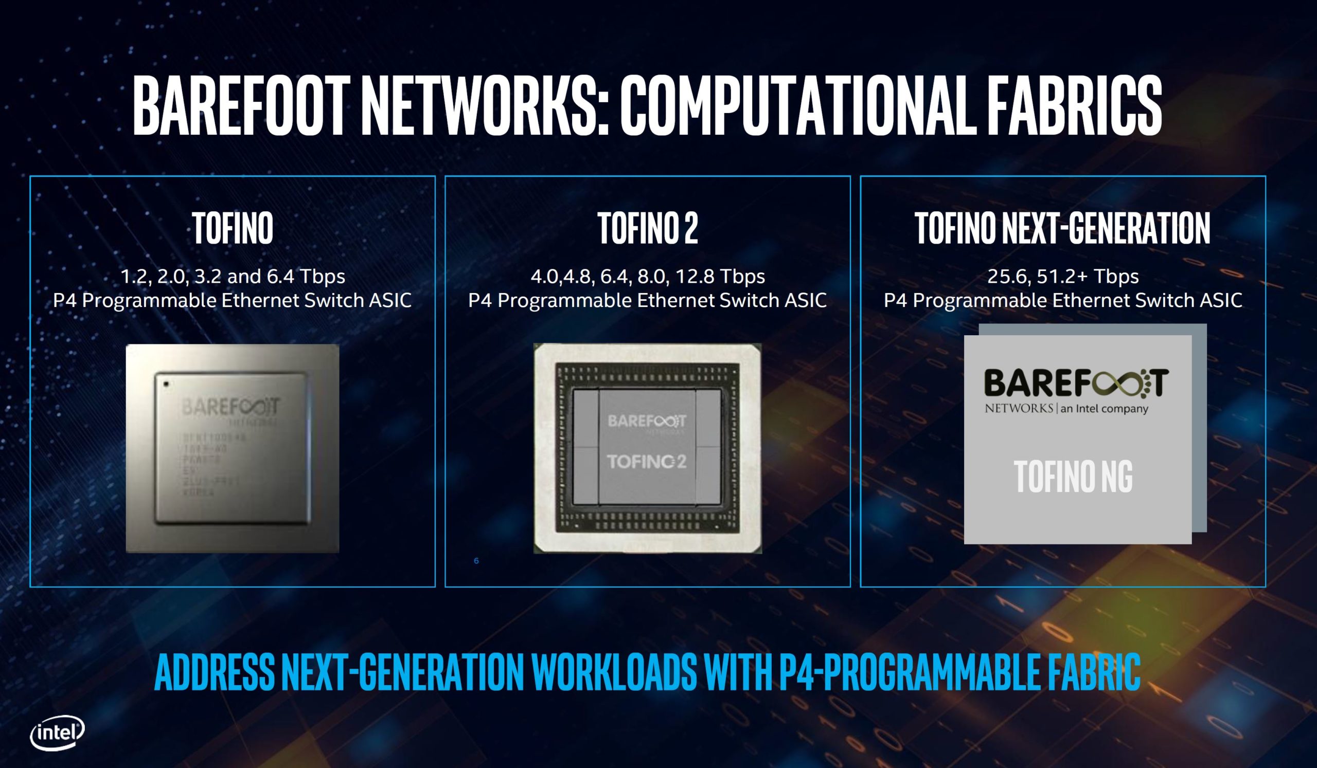
On the Barefoot side, something interesting that many may not have known is that this that the Tofino 2 is not a single monolithic die. Instead, there is the main switch ASIC silicon flanked by four I/O die chips using TSMC 7nm packaging technology. When we recently featured an Edgecore AS7712-32X switch that was a 3.2Tbps device based on another vendor’s silicon. Barefoot Tofino (gen 1) supported up to 6.4Tbps. Tofino 2 used in the silicon photonics technology demo can scale up to 12.8Tbps. The next-generation products will scale to 25.6 and 51.2Tbps.
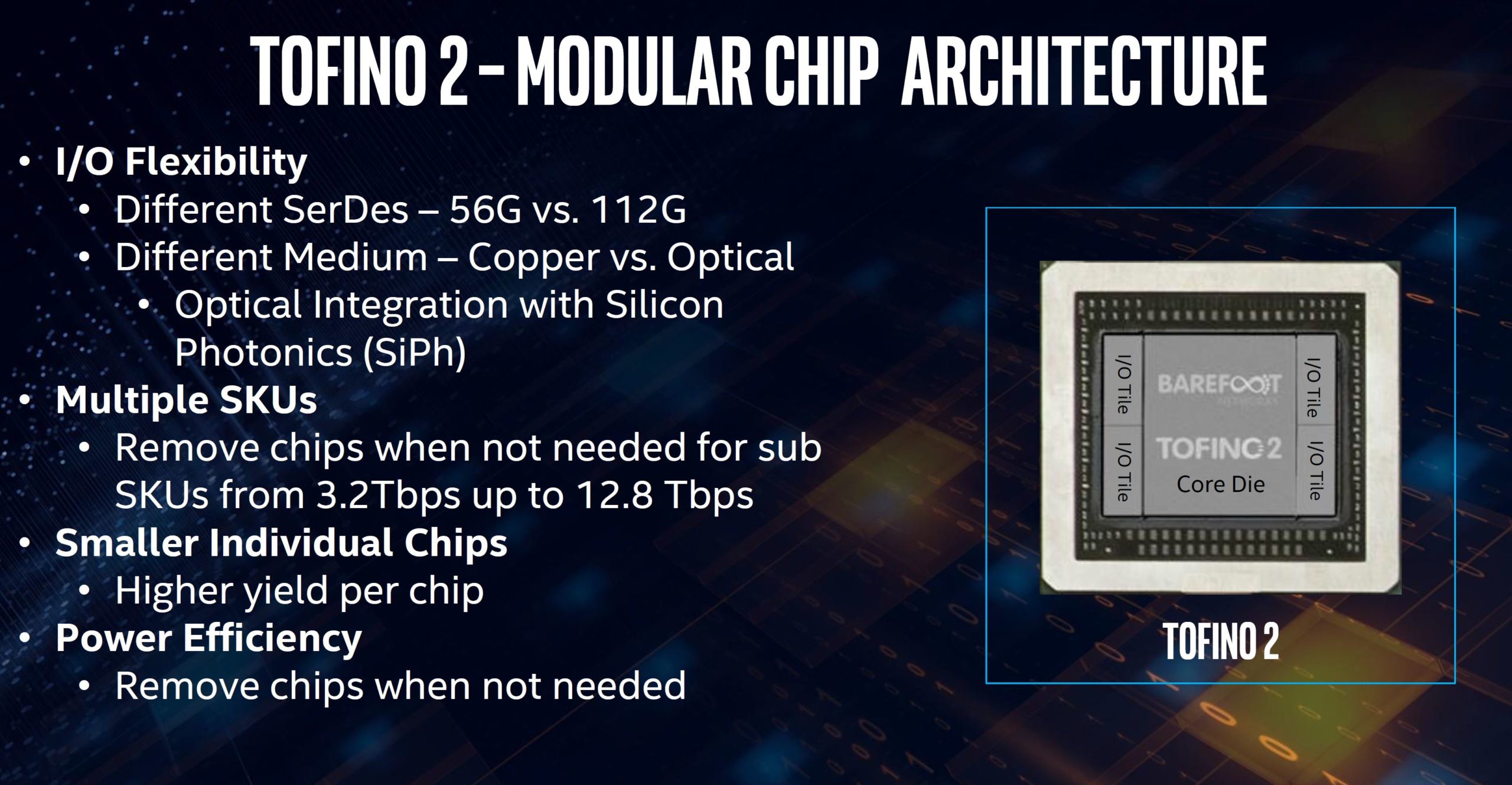
With the modular architecture, one could imagine the day when the I/O die has silicon photonics and there is no need for external packaging.
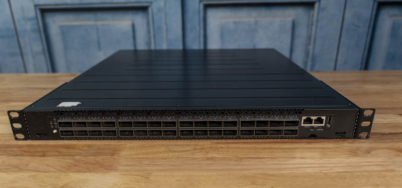
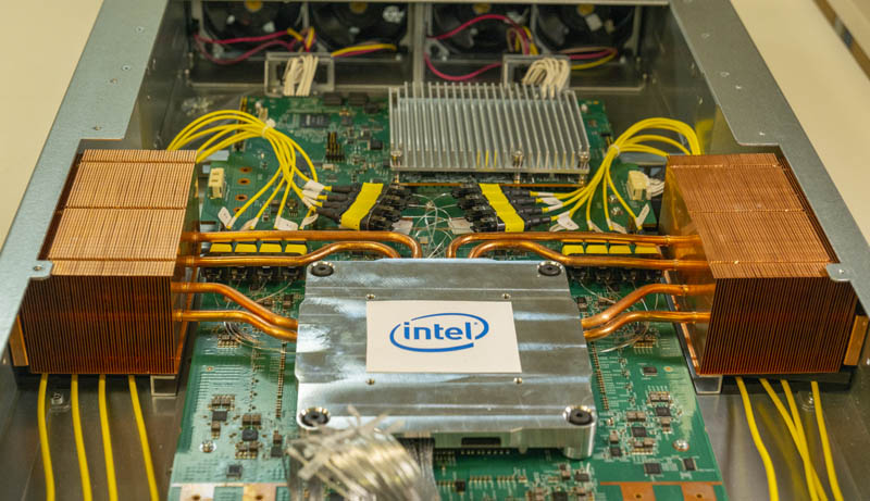
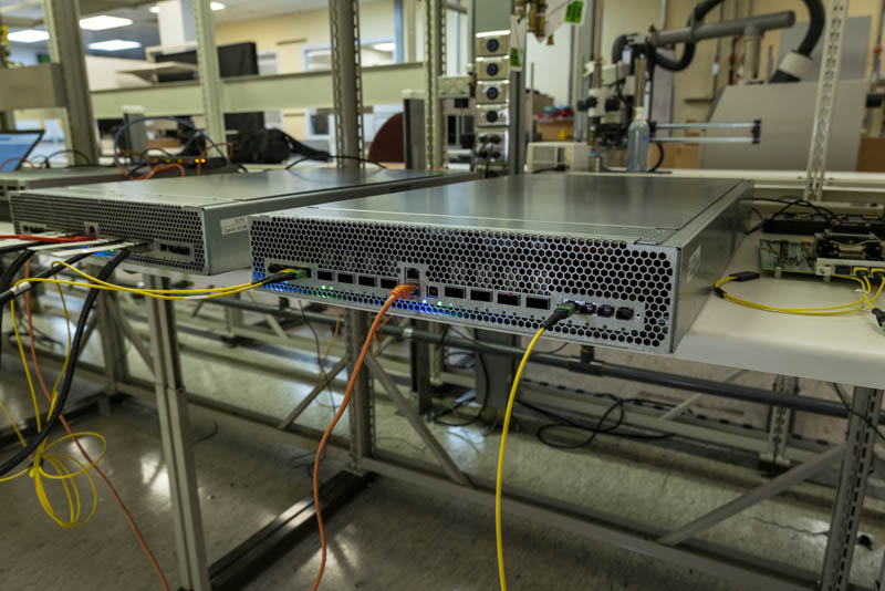
The demo itself utilizes this Tofino 2 chip with co-packaged optics. Optical modules are placed on a LGA package that then sits in sockets surrounding the main switch chip. Fiber is attached to these silicon photonics modules and used to connect to the faceplate MTP optical connectors.
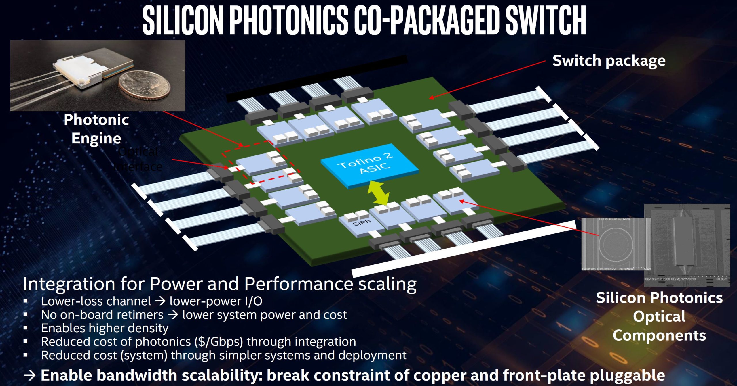
What that diagram shows is that data is traveling a very short distance between the switch ASIC and co-packaged silicon photonics engines. The strands coming out of the optical engines are then mated inside the chassis to the front panel MTP connectors. This gives more deployment flexibility and helps move data away from the switch ASIC. Normally, there is a large copper block atop the switch chip covering this area.
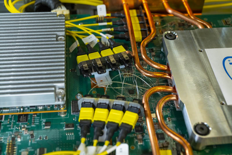
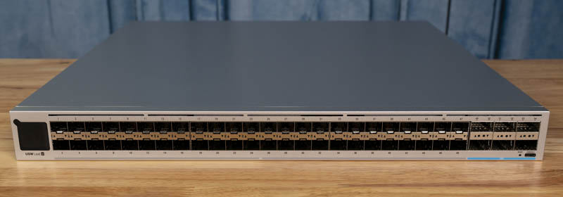
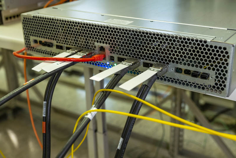
The demo switches not only have silicon photonics packages, but Intel is actually showing off some flexibility here as well. Each of the three test switches we saw (based somewhat on the Facebook Wedge platform) all included copper connectivity as well to standard QSFP cages.
Key here is that using these packages around the switch chip gives customers the ability to specify to switch vendors that four traditional pluggable cages are required while the rest of the switch should be half short-range and half long-range optics.
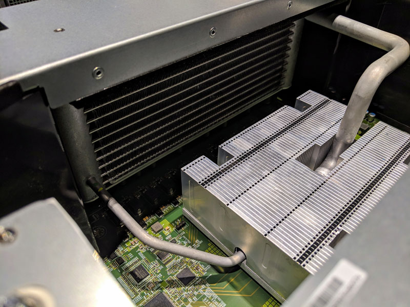
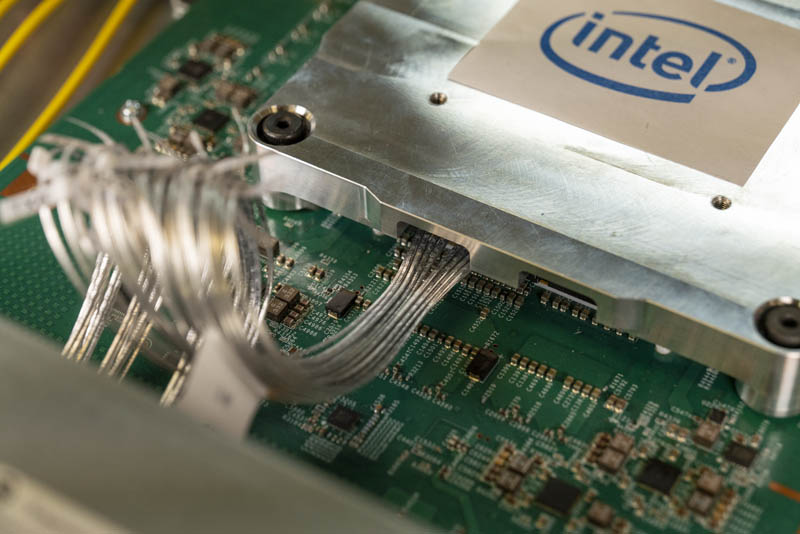
During my time in the lab, I was able to see underneath the metal block covering the assembly. There is IP there that Intel is not ready to share so I was not allowed to take photos of that view. At the same time, it was one of those solutions that once you see it it becomes readily apparent how switch vendors such as Cisco, Arista, Quanta, and others will be able to customize switches for customer requirements. One can also see that these packages, even if reliable, are also something that can be serviced should they fail, although that may be a send to factory service since there is a massive cooling solution on the switch chip.
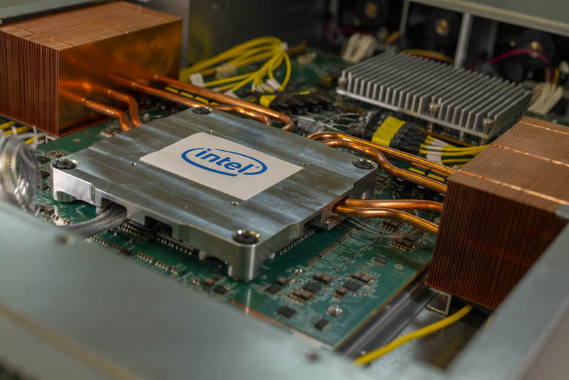
I was also not allowed to take pictures of the heatsink assembly that was removed in Intel’s demo unit. It is a big all-copper heatsink that fills the void between the two heatsinks on either side of the switch that Intel is showing. if you see those heat pipes and copper coolers in the demo unit, those are not for the switch ASIC. Instead, they are designed to cool the silicon photonics packages.
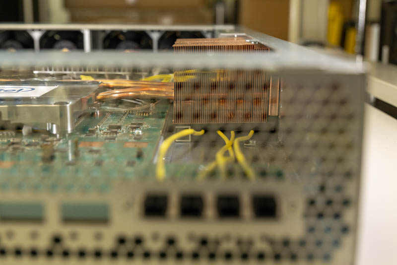
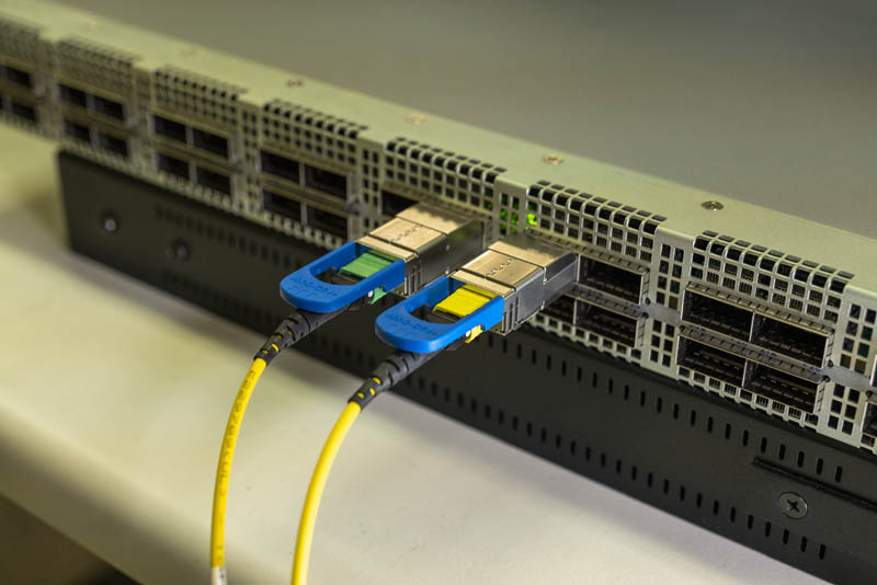
On the subject of cooling, you can see how much smaller the MTP connectors at the front of the switch are compared to the QSFP cages. That allows more unobstructed faceplate room for airflow providing more efficient cooling.
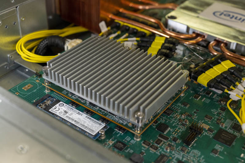
For the control plane, we can see the daughtercard with the Intel Xeon D control plane CPU.
Intel had another demo setup with an existing Arista switch pumping data through the silicon photonics co-packaging switch.
The Arista switch was using another vendor’s silicon so this is interesting since it is also showing an interoperability demo, important in the networking space. For those that saw the pictures when Intel released them, this is not just a mechanical demo, this is passing traffic to other Barefoot switches as well as working linked to switch silicon from other vendors.
That demo was being monitored by the notebook PC found in the far left of this photo. Essentially that is simply showing traffic passing through the different switches to prove that the chain is working.
Final Words
The impact of this can be huge. We heard this can yield a 20-30% power savings in next-generation switches. Shortening the distances between where the signal originates and terminates on the switch chip to the optical transceiver is a big opportunity to gain efficiency in the data center. If you are a public cloud provider such as Amazon, Microsoft, Google, or Alibaba and have data center level power constraints, eliminating networking power can be a big win. These pubic cloud providers generally are selling compute resources, not networking. As a result, lowering the networking power consumption allows these companies to increase the ratio of compute in the data center which is essentially a public cloud provider’s saleable unit.
At 12.8Tbps this co-packaging technology is not needed. By the time we hit 51.2Tbps, something like this will be necessary. What Intel is showing off, and from what I saw underneath the covers, the current state of the technology is not a lab-only solution. Unlike some Intel demos I have seen, or the packaging study shown at OCP Summit in 2018, this is something a switch vendor like Quanta could pick up and by the end of 2020 turn it into a saleable product. The need may not be there, but the technology maturity level is much higher than I was expecting from the initial photos.
Since OFC and other conferences are canceled for the time being, we are going to do more of these exhibition floor alternative pieces. Hopefully, this provides you with some idea of what would have been shown on the OFC floor and more importantly where the industry is today and where it is headed. This is a trend that will happen because there is a market need and the market makers are pushing for it. A few years ago this was conceptual only. Today, it is hitting the point where it could be productized relatively quickly as the key components are functioning.


@Patrick, I get from this that the optics is moved from the QSFP plug to electro-optical chips locatrd very near the big switch chip.
But the front of the switch still seems to be all QSFP sockets. Why don’t they use smaller little plastic connectors for the fibre optic cables?
Emereth – shown in some of the pictures. The test switches have both traditional cages (inner ports) and MTP connectors (outer ports.) The MTP connectors are much smaller.
Patrick – thanks!
Hi @Patrick,
In terms of 400G SiPh solution, Intel seems to use the same 4-channel architecture as its 100G transceivers, just now increasing to 100G per channel from 25G per channel through drivers/modulators/MEMS technology.
What does that mean to the laser itself? Are these lasers larger in die per channel? If so, how much larger on average, and if not, are they using basically the same exact 25G InP laser with added silicon ICs to boost the throughput?
Comments are closed.