
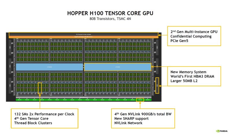
At Hot Chips 34, NVIDIA is sharing more details on its Hopper GPU. The NVIDIA H100 known as a “Hopper” generation part, is the company’s first PCIe Gen5 era data center GPU with a host of improvements.
Note: We are doing this piece live at HC34 during the presentation so please excuse typos. This is being done much faster than my normal pieces so I will apologize here for it, but it may be worthwhile to read slides here.
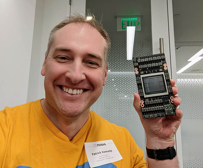
NVIDIA H100 Hopper Details at HC34
The NVIDIA H100 is fabbed on TSMC 4N and is over 80B transistors on a monolithic die. This is a big chip. It also uses HBM3 and has a 50MB L2 cache. We are going to hear more about caches from Intel and AMD.
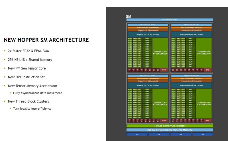
The new Hopper SM has a new instruction set called DPX in this generation. There is also a new Tensor Memory Accelerator, and Thread Block Clusters. We will get to those soon.
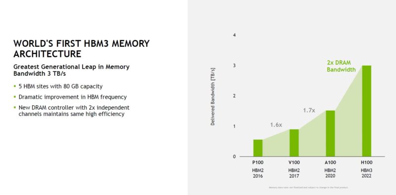
There are five HBM3 sites on the H100 (although you can see six, one is structural. HBM3 adds a lot of memory bandwidth in this generation hitting 3TB/s.
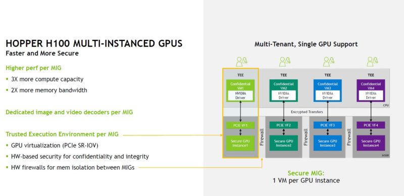
One of the big changes in this generation is better security but also more capabilities to the H100’s Multi-instance GPU (MIG.) NVIDIA’s idea is that one can buy H100’s for the data center/ cloud, and then parse them into smaller slices. This is a big upgrade versus what we have seen in the A100 generation.
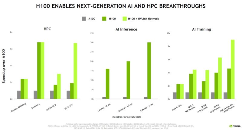
This is perhaps the easiest one to explain, NVIDIA has a new generation of technology and it is faster than its old (current) one.
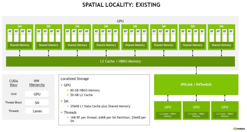
We are not going to cover all of the data locality and asynchronous execution parts of the talk, but spacial locality is one of them. An example is a spacial locality where in CUDA spacial locality can be expressed as a grid. Then, locality can be thread blocks, then threads. NVIDIA takes a grid of work, then chunks the work to these resources to minimize data movement.
NVIDIA says that in 10 years it has had an order of magnitude level of complexity.
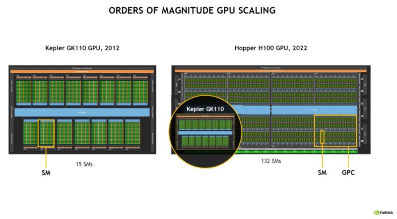
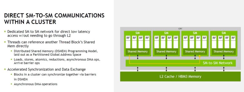
With the NVIDIA H100, there is now a thread block cluster that adds a new level to the locality hierarchy. This is required because the GPUs have scaled to such large complexes that there needs to be another level.
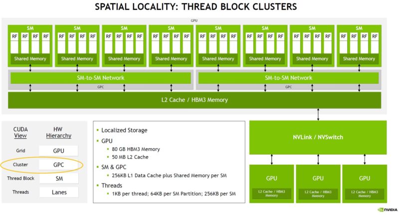
The thread block has a direct SM-to-SM network that helps data movement in the cluster. This locality means that data transfer is more localized and thus is more efficient. We will let you read this slide.
NVIDIA also discussed temporal locality and its thread block reconfiguration.
Another area that NVIDIA discussed the H100 was asynchronous computation. The NVIDIA H100 is designed to work in an asynchronous manner. Instead of threads having to wait for data and pause, threads can complete at different rates. You can look up NVIDIA’s asynchronous transaction barrier for more information on it.
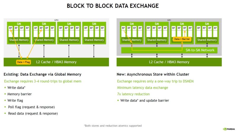
NVIDIA showed the impact of A100 to H100 block data exchange. NVIDIA says the new async transactions can yield up to a 7x latency improvement. There is also a new TMA to help copy data within the thread block clusters and also to caches and memory.
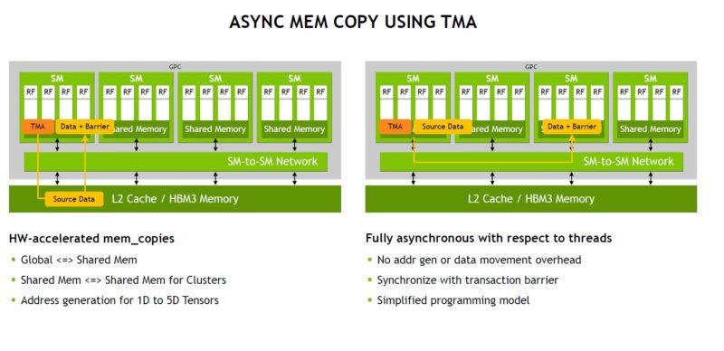
TMA takes away a lot of the work for moving memory from threads to allow them to do higher-value tasks.
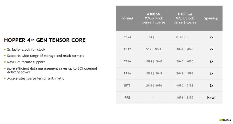
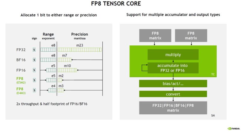
NVIDIA H100 Hopper 4th Gen Tensor Core and FP8
Hopper not only doubles the performance of the previous generation but also has FP8 data types.
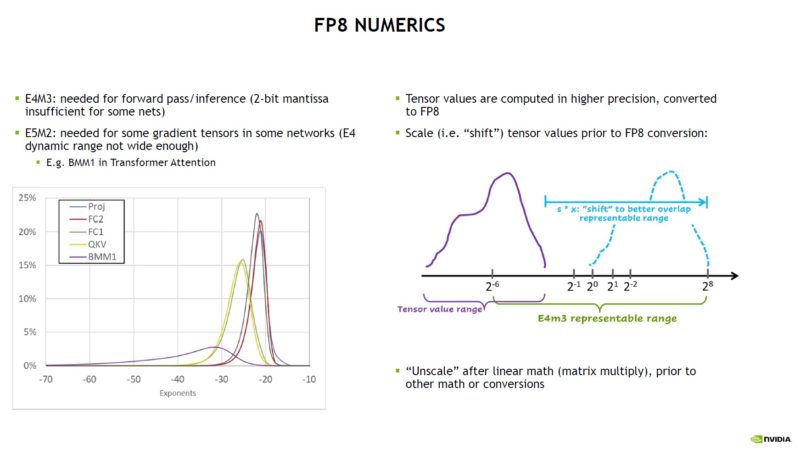
There are both FP8 E5M2 and E4M3 formats. There are two different versions, and we have covered them previously in our NVIDIA GTC 2022 Keynote Coverage.
Here is what NVIDIA found as a driver for the E5M2 and E4M3 FP8 formats.
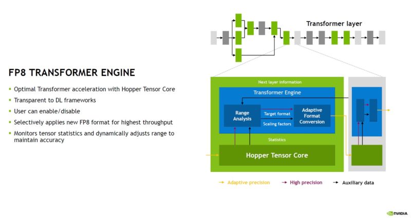
The Hopper FP8 Transformer Engine analyzes statistics on which FP8 format is best for a given problem. It can also apply the right format to each layer.
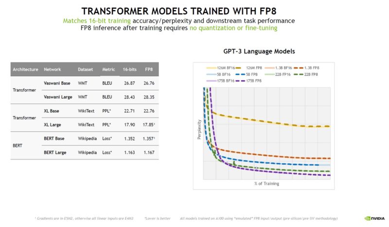
Here, NVIDIA shows that it is getting similar accuracy with FP8 versus FP16. The implication is that it is roughly twice as fast.
This was a rapid-fire presentation and was very hard to cover live.
Final Words
NVIDIA’s biggest challenge with Hopper is not just making the GPU. It also needs PCIe Gen5 platforms to be released so it can start selling the new GPUs. We have already spotted them in the wild, but with delays to the expected timelines for Intel Xeon Sapphire Rapids and AMD EPYC Genoa, NVIDIA has a GPU that needs a host platform. That is a big driver behind Grace.
Still, we cannot wait to get the NVIDIA H100 in the lab since every new generation is a new step into more performance. Also, NVIDIA has a great software ecosystem making these GPUs relatively easy to use compared to some of the other solutions out there.


Is the DGX / HGX H100 internally liquid cooled? On the first picture it appears that there are no heatsinks on the GPUs. Is there already any information on that?
Would at least make sense for those 700W beasts.
Comments are closed.