
At Hot Chips 34, AMD talked a bit more about making its MI250X GPU and the system topologies with it. We first saw the AMD Instinct MI250X OAM at SC21 and since then HPE and AMD Powered Frontier Tops the Top500 Ushering in Exascale. This is the GPU and systems architecture powering the #1 Top500 supercomputer today.
Note: We are doing this piece live at HC34 during the presentation so please excuse typos.
AMD MI250X and CDNA 2 HC34
AMD has its floorplan of the MI250X. This is 58B in 6nm TSMC. The NVIDIA H100 is 80B in N4. Here we get the key features like the 128GB of HBM2e, the PCIe/ Infinity Fabric links, coherent links to the CPU, and more. Between the two GPUs on the MI250X, there is a 400GB/s link on the OAM package. The PCIe link allows a NIC to be directly attached to each side of the GPU.
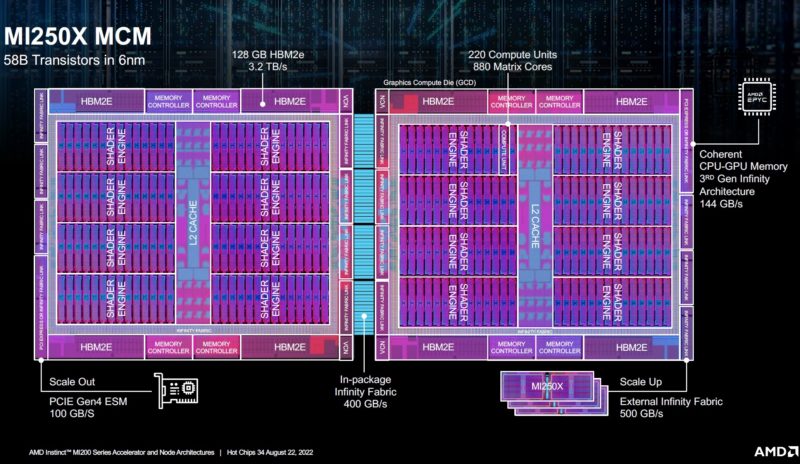
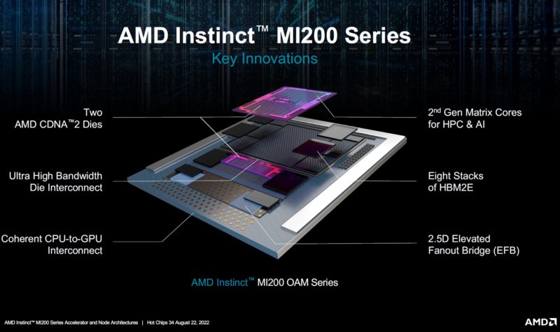
Just to keep things in perspective, the MI250X is a single OAM package, but it is effectively two GPUs tied together. When you see “eight stacks of HBM2E” the way to think of this is that each GPU die has four of them. AMD says the total package is 10 chips and uses an elevated fan-out bridge.
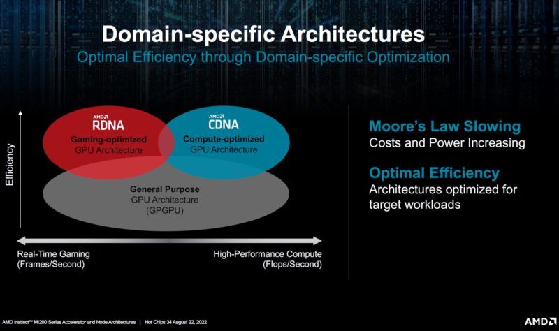
AMD also split its GPU architectures into RDNA for graphics and CDNA for CPU compute. We call the MI250X a GPU, but perhaps it is more like a GPU compute architecture.
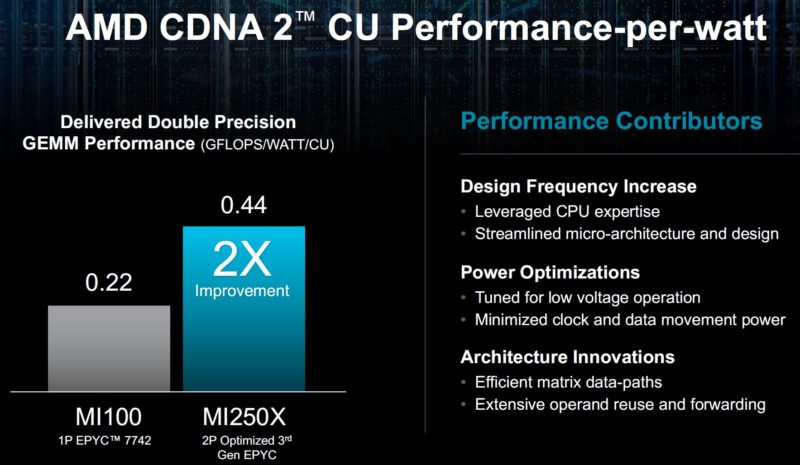
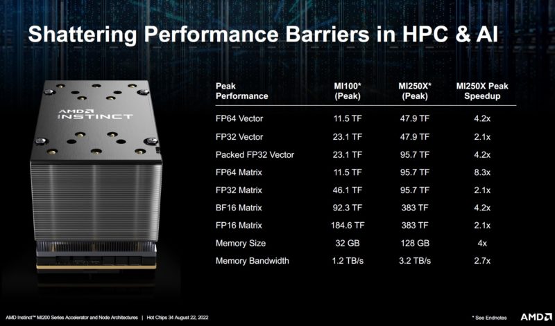
Between the CDNA optimization, along with the new improvements in CDNA2, it gets around twice the performance per watt on double precision workloads than the MI100 generation.
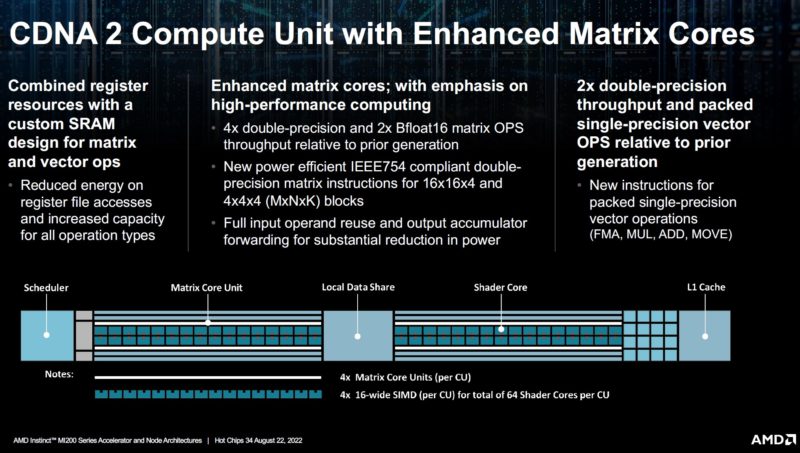
With CDNA 2, each compute unit gets a matrix core unit as well. This matrix compute feature is at a high level similar to other matrix math features from companies like NVIDIA and Intel. AMD has a different implementation that was designed to drive efficiency as well as performance.
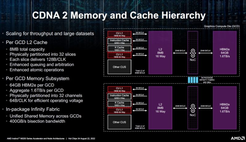
A major implementation detail is also how the L2 cache and the memory works. Here each GCD gets 8MB of L2 cache. The L2 cache design is needed to feed the compute units with data.
We have seen this before, but AMD says that its new version is faster than its old version. What is also interesting here is that AMD has effectively two co-packaged GPUs with the MI250X. So only a 2x speedup feels more like having more GPUs.
AMD’s 3rd generation Infinity Architecture looks very cool in the photo, but what it effectively does is map an AMD EPYC 7003 Milan CCD to one of the GPU halves on the MI250/ MI250X.
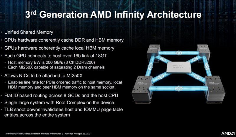
The biggest theme we hear about from AMD is minimizing data movement.
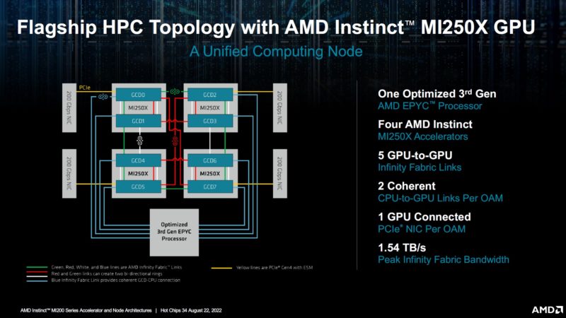
Building Systems with AMD MI250X and MI250 OAM GPU Topologies
This is the HPC topology from AMD that is being used in Frontier. AMD says that the EPYC is customized, but has not provided much on what those customizations are.
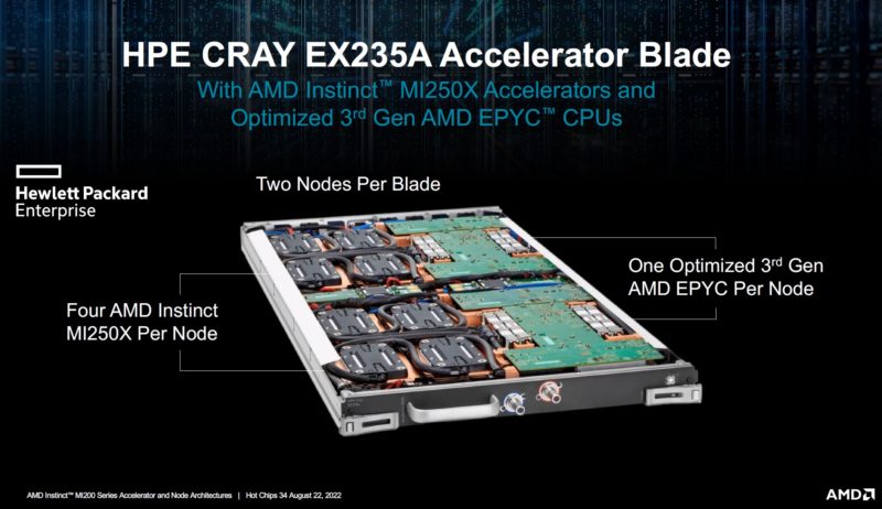
The HPE Cray EX235a is the node that is powering modern supercomputers.
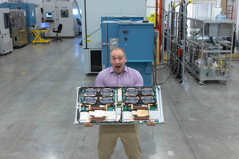
You may have also seen this in our Top 10 Showcases of SC21 piece as well as our How Liquid Cooling is Prototyped and Tested in the CoolIT Liquid Lab Tour. These nodes are heavy!
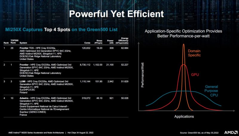
The AMD-HPE blade has the #1 and #3 spots on the Top500 list and leads on the efficiency-focused Green500 as well.
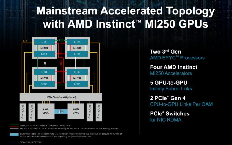
AMD has a PCIe Gen4 compatible platform using PCIe switches. The PCIe switches are used for RDMA network transfers.
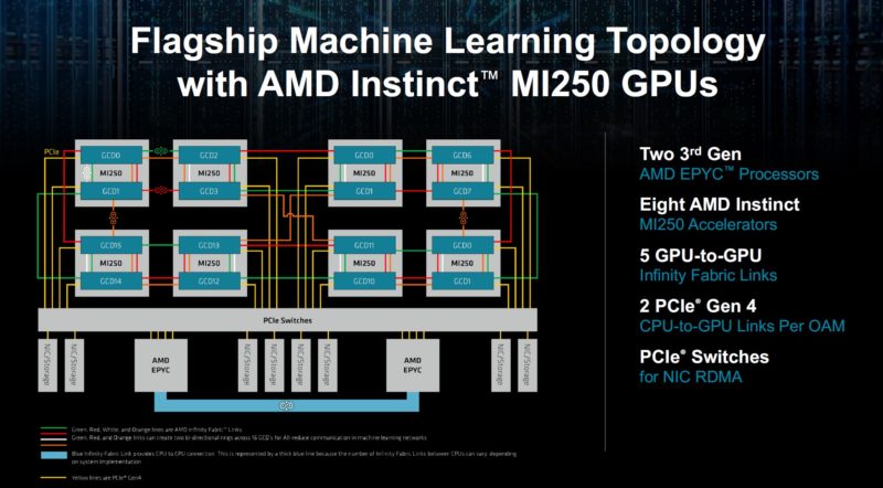
AMD also has an AMD Instinct MI250 machine learning topology. This has 8x GPUs and 2x EPYC CPUs.
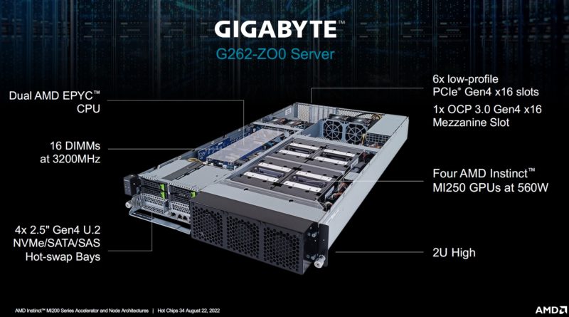
Gigabyte has a mainstream topology 2U server called the G262-ZO0.
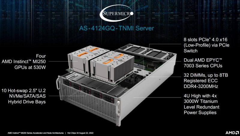
The Supermicro AS-4124GQ-TNMI is also a mainstream topology MI250 server.
This is very interesting since they should be in similar power envelopes to the Dell EMC PowerEdge XE8545 and Supermicro SYS-220GQ-TNAR+ Redstone platforms we have looked at.
Final Words
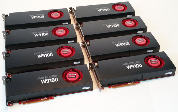
This is a very cool presentation. We have been watching the MI250X and MI250 progress for a few years now, into running the #1 Top500 supercomputer. In the background, we are also working on getting some AMD GPU content online. Stay tuned for AMD GPU server reviews that may be the first since we did the 2015 ASRock Rack server review with 8x AMD FirePro GPUs!
AMD has sure come a long way since then!

