
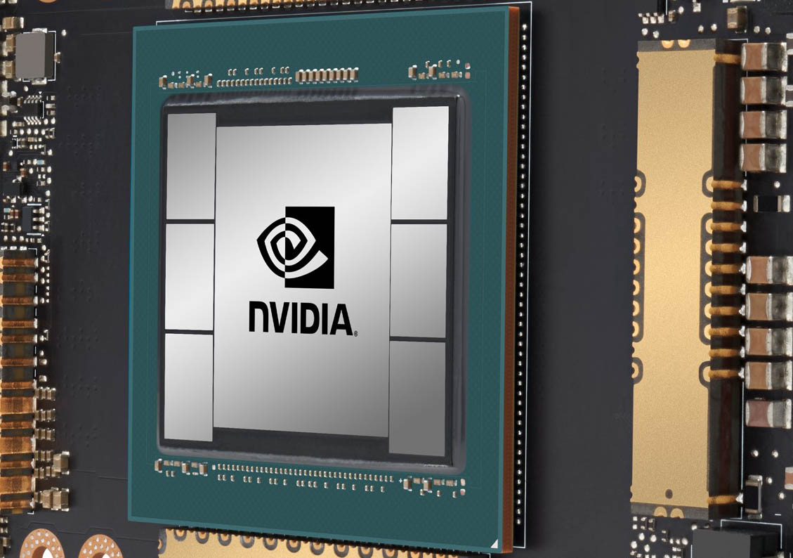
Since its release in 2017, the NVIDIA Tesla V100 has been the industry reference point for accelerator performance. Intel compares its CPUs and AI accelerators to Tesla V100 GPUs for HPC workloads. Every AI company measures its performance to the Tesla V100. Today, that measuring stick changes, and takes a big leap with the NVIDIA A100. Note the cards are actually labeled as GA100 but we are using A100 to align with NVIDIA’s marketing materials.
NVIDIA A100 Key Specs
Let us start with the A100 key specs:
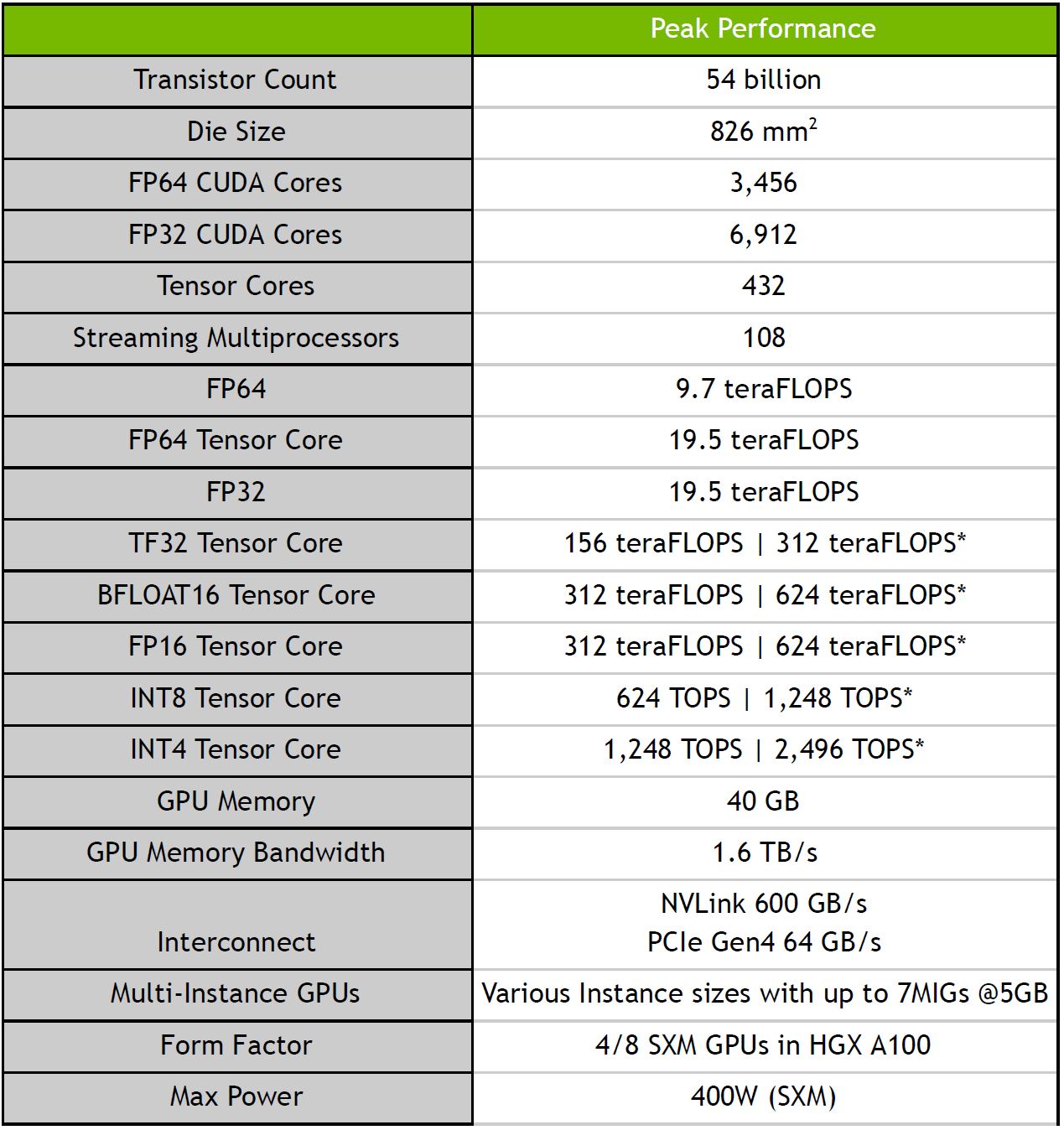
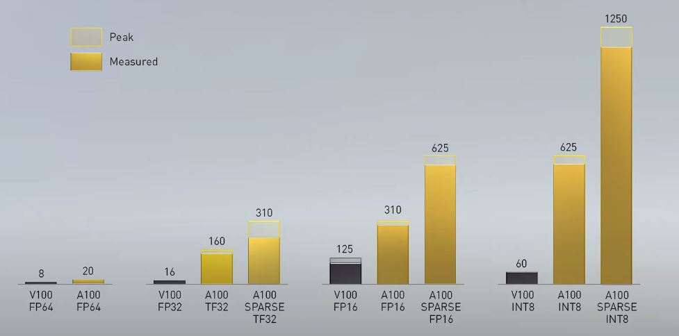
You may ask yourself, what are the asterisks next to many of those numbers, NVIDIA says those are the numbers with structural sparsity enabled. We are going to discuss more of that in a bit. Here is the peak v. measured for Tesla V100 v. A100 that NVIDIA is showing.
Let us dive into some of these details to see why they are impactful.
NVIDIA A100 (SXM) Details
NVIDIA is inventing new math formats and adding Tensor Core acceleration to many of these. Part of the story of the NVIDIA A100’s evolution from the Tesla P100 and Tesla V100 is that it is designed to handle BFLOAT16, TF32, and other new computation formats. This is exceedingly important because it is how NVIDIA is getting claims of 10-20x the performance of previous generations. At the same time, raw FP64 (non-Tensor Core) performance, for example, has gone from 5.3 TFLOPS with the Tesla P100, 7.5 TFLOPS for the SXM2 Tesla V100 (a bit more in the SXM3 versions), and up to 9.7 TFLOPS in the A100. While traditional FP64 double precision is increasing, the accelerators and new formats are on a different curve.
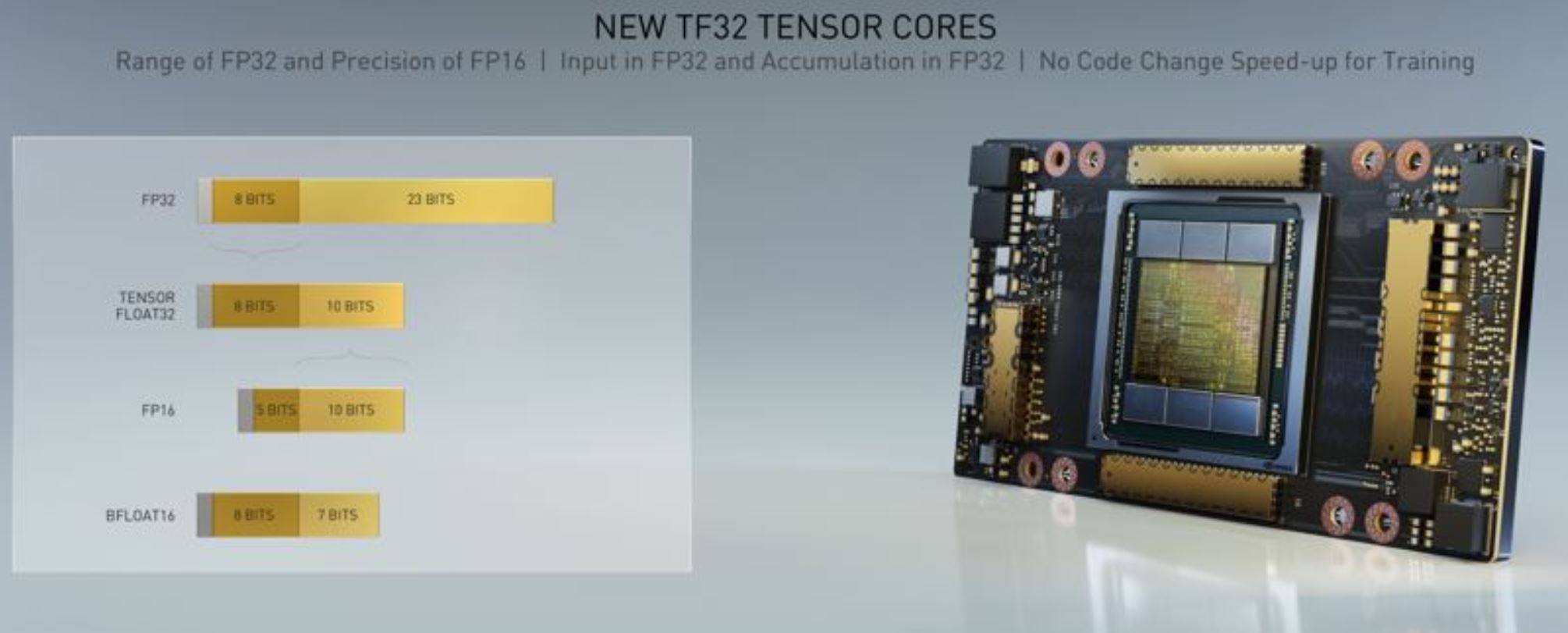
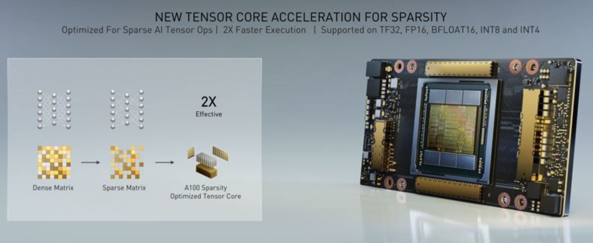
Both BFLOAT16 and TF32 are numerical formats that retain acceptable accuracy while greatly reducing the bits that are used. Lower bits in each number mean less data needs to be moved and faster calculations. Those new formats are augmented by Tensor Cores and structural sparsity. With structural sparsity, the A100 can take advantage of sparse models and avoid doing unnecessary computations. You can read the presentation on structural sparsity here.
Memory has gone from 16GB of HBM2 on the Tesla P100 to 16GB and 32GB on the Tesla V100 and now 40GB. That is a jump, but a more measured jump. A few folks reached out asking why it looks like the A100 package has six Samsung HBM2 stacks but the total is not divisible by 6. Perhaps NVIDIA is planning a 48GB version in the future or there is something else going on. We will update if more details emerge than we have while writing this (before the keynote is live.) Memory bandwidth is up to 1.6TB/s.
As a quick note, on the pre-keynote briefing, Jensen Huang, CEO of NVIDIA hinted that there is a reason NVIDIA does not use HBM2 on its consumer GPUs. He did not say it, but it is likely cost. As a result, we would not expect HBM2 in the next GeForce GPUs.
For die size, the 54B transistor GPU measures 826mm2 and is built on TSMC 7nm. This is a big process shrink that helps NVIDIA pack in much higher densities for more compute. Even with the 7nm shrink, power is going up, now rated at 400W. In our recent Inspur NF5488M5 Review A Unique 8x NVIDIA Tesla V100 Server we noted that “Volta-Next” (e.g. A100) support would be at 400W. Currently, the DGX-2h rates its Tesla V100’s at 450W so our sense is that 400W is not the highest level we will see. Also, this is for the SXM variants. PCIe cards will still be limited by thermals so we expect lower power there.
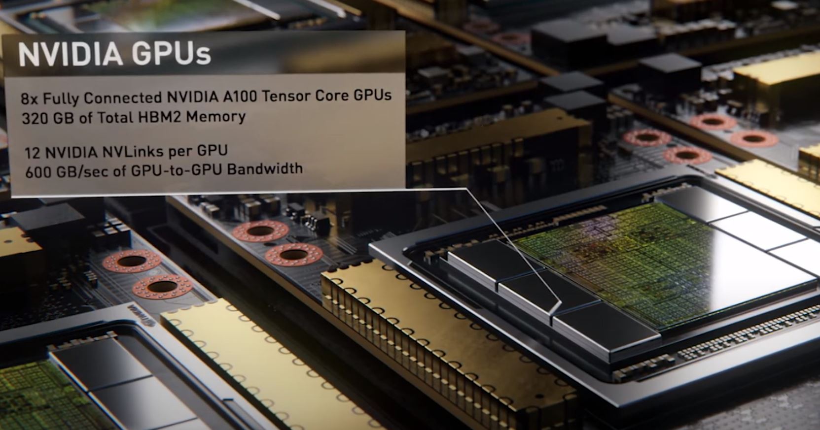
NVLink speeds have doubled to 600GB/s from 300GB/s. We figured this was the case recently in NVIDIA A100 HGX-2 Edition Shows Updated Specs. That observation seems to be confirmed along with the PCIe Gen4 observation.
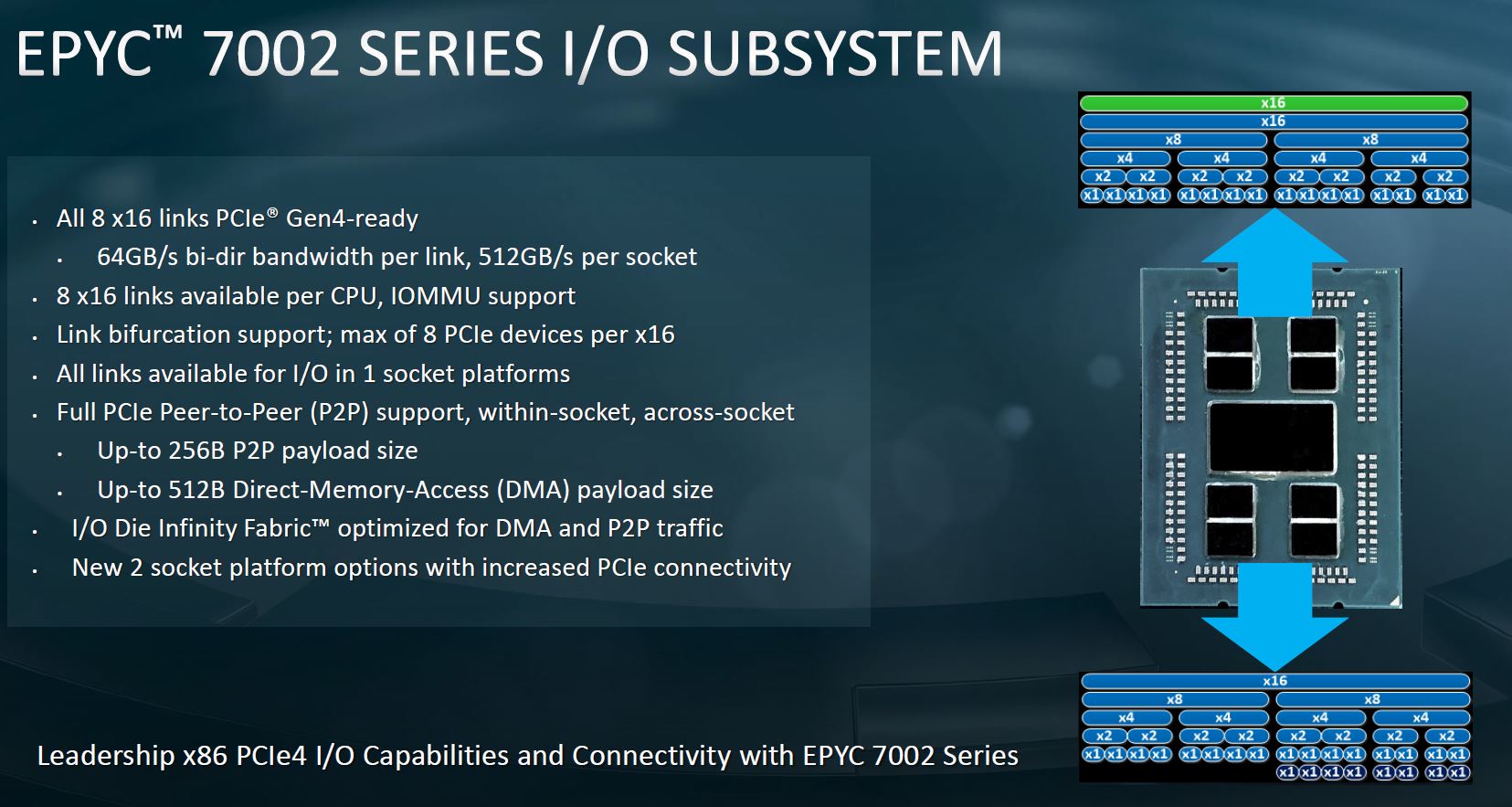
The A100 now utilizes PCIe Gen4. That is actually a big deal. With Intel’s major delays of the Ice Lake Xeon platform that will include PCIe Gen4, NVIDIA was forced to move to the AMD EPYC 64-core PCIe Gen4 capable chips for its flagship DGX A100 solution. While Intel is decisively going after NVIDIA with its Xe HPC GPU and Habana Labs acquisition, AMD is a GPU competitor today. Still, NVIDIA had to move to the AMD solution to get PCIe Gen4. NVIDIA’s partners will also likely look to the AMD EPYC 7002 Series to get PCIe Gen4 capable CPUs paired to the latest NVIDIA GPUs.
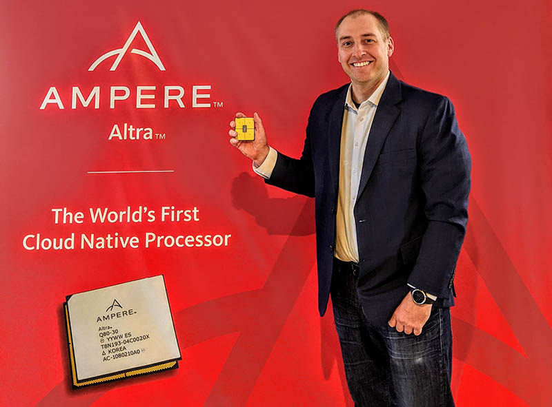
NVIDIA wanted to stay x86 rather than go to POWER for Gen4 support. The other option would have been to utilize an Ampere Altra Q80-30 or similar as part of NVIDIA CUDA on Arm. It seems like NVIDIA does not have enough faith in Arm server CPUs to move its flagship DGX platform to Arm today. This may well happen in future generations so it does not need to design-in a competitor’s solution.
Multi-Instance GPUs (MIG) are a feature that when you hear about it makes a lot of sense. With this feature, NVIDIA can take an A100 and split it up into as many as seven partitions. Each MIG gets its own dedicated compute resources, caches, memory and memory bandwidth. For cloud providers, they have less incentive to use different GPUs and more incentive to deploy the A100 and partition it into smaller chunks. While the compute resources will go up significantly, the memory available to MIGs will likely be less than the 32GB on a Tesla V100.
What Is the Supply Situation?
I was able to ask Jensen a question directly on the obvious question: supply. Starting today onward, a Tesla V100 for anything that can be accelerated with Tensor Cores on the A100 is a tough sell. As a result, the industry will want the A100. I asked how will NVIDIA prioritize which customers get the supply of new GPUs. Jensen said that the A100 is already in mass production. Cloud customers already have the A100 and that it will be in every major cloud. There are already customers who have the A100. Systems vendors can take the HGX A100 platform and deliver solutions around it. The DGX A100 is available for order today. That is a fairly typical data center launch today where some customers already are deploying before the launch. Still, our sense is that there will be lead times as organizations rush to get the new GPU for hungry AI workloads.
With the first round of GPUs, we are hearing that NVIDIA is focused on the 8x GPU HGX and 4x GPU boards to sell in its own and partner systems. NVIDIA is not just selling these initial A100’s as single PCIe GPUs. Instead, NVIDIA is selling them as pre-assembled GPU and PCB assemblies.
Final Words
The NVIDIA A100 is a first step for the new GPU. When one looks at the Tesla V100 there are a number of options including:
- Single-slot PCIe 150W 16GB version
- Dual-slot PCIe 16GB
- Dual-slot PCIe 32GB
- Dual-slot PCIe 32GB (V100S)
- SXM2
- SXM3 (350W)
- SXM3 (450W) for the DGX-2h
With at least seven different variants that use the “Tesla V100” label, NVIDIA has some market segments to fill. We expect some segments to perhaps go away this cycle but also new ones such as the EGX A100 we are covering today to be introduced. In the pre-brief for today’s announcement, NVIDIA offered that Ampere inferencing performance is so high that it will supplant Tesla T4’s. While this is likely to happen, at 400W the current iteration will not fit in edge use cases that need lower power envelopes. We look forward to seeing the A100 line fill-out over the coming quarters.
You can check out our piece on how these GPUs are used in our NVIDIA DGX A100 Leapfrogs Previous-Gen piece.
Note: We got late word that this is now the NVIDIA A100 without the “Tesla” branding.


The choice of AMD is telling – Nvidia sees more of a safe port with AMD – while they will be dealing with Intel getting into the GPU business… So seems that Nvidia sees Intel as a much bigger threat than AMD in the GPU space.
Intel is not going after AMD with its Xe HP and HPC lines – it’s Nvidia. Deep pockets can overcome alot of the issues with converting people and shops from CUDA to Intel. Intel is about the only company that can pierce the Nvidia ecosystem – which has been built up over years. When you factor in the Habana products and the FPGA line (Agilex) – combined with CXL… it’s going to get interesting.
Intel’s dominant position in the DC will make dethroning Nvidia quite a bit easier – and in hyper scale / heavy AI environments, it will be a blood bath.
Interesting times ahead.
In the meantime it’s Frontier and El Capitan for the U.S. Department of Energy.
Intel is still using 14nm+++++++++++++++++++, PCIe3 and hiring everyone to become a techcompany again. Cray has Slingshot, NVidia has Mellanox and intel has ???. Xilinx is also not sitting still and findings ways to counter former Altera. Intel will come back, the neural chip is promissing, guess we have to wait and see what 2022/23 brings.
Is it big? Sure! Is it fast? Sure!
But is it as impressive as presented? I am not so sure, take the dated vega20 chip which is built on the same process for comparison. A100 has more than 2.5x the die size, yet less than 1.5x the perf of vega20.
@Bob Dobbs cool story… But the reason nvidia is going with EPYC is intel doesn’t have anything other than inferior garbage for the foreseeable future. They don’t have the perf, they don’t have the cores, they don’t have the IO. All they have is an ever increasing mess of security issues.
As for intel’s latest GPU aspirations, leaked insider information suggests it is nothing but tragedy. Time will tell, yet I won’t be holding by breath for intel making a decent gpu, much less for selling it at a decent price.
Intel is notoriously bad at anything outside the field of its PC cpu monopoly. They have a long history of failures, and the only decent products they added to their portfolio came not from in-house development, but by buying existing companies that already had decent products. I don’t recall intel buying a GPU company lately, all they really have is a mediocre iGPU architecture and Raja the diversity hire goat, who’s previous employment at AMD led to a total fiasco.
This certainly do not look good for intel and their gpu, which also explains why they don’t have anything other than hype, and they are going well beyond excessive on it.
It’s not clear: do we get a unified flat common address space? Or is it still some sort of RDMA layered over with sotware?
I’m confused by the sparsity HW. Apparently it is only useful during inference as it isn’t clear which weights are going to be important during training. So why store the unimportant weights in memory during inference? What am I missing here?
Intel is certainly bigger threat to Nvidia than AMD. I would ignore the AMD fanboy noise here, its getting bit ridiculous. Obviously Nvidia tries to weaken Intel by going AMD as Nvidia sees AMD as no threat at all. They’ve always managed to defeat AMD GPUs with ease. Not to mention AMD has no real data center moat or ecosystem the way Intel does. Intel’s 14nm+++++ or whatever it is, is actually better than TSMC 10nm. So they’re not that far behind as AMD fanboys want people to believe. Intel 10nm likewise is better than TSMC 7nm, Intel 7nm better than TSMC 5nm. Not to mention nm itself is just marketing term, its transistor density that defines better process node.
Comments are closed.