
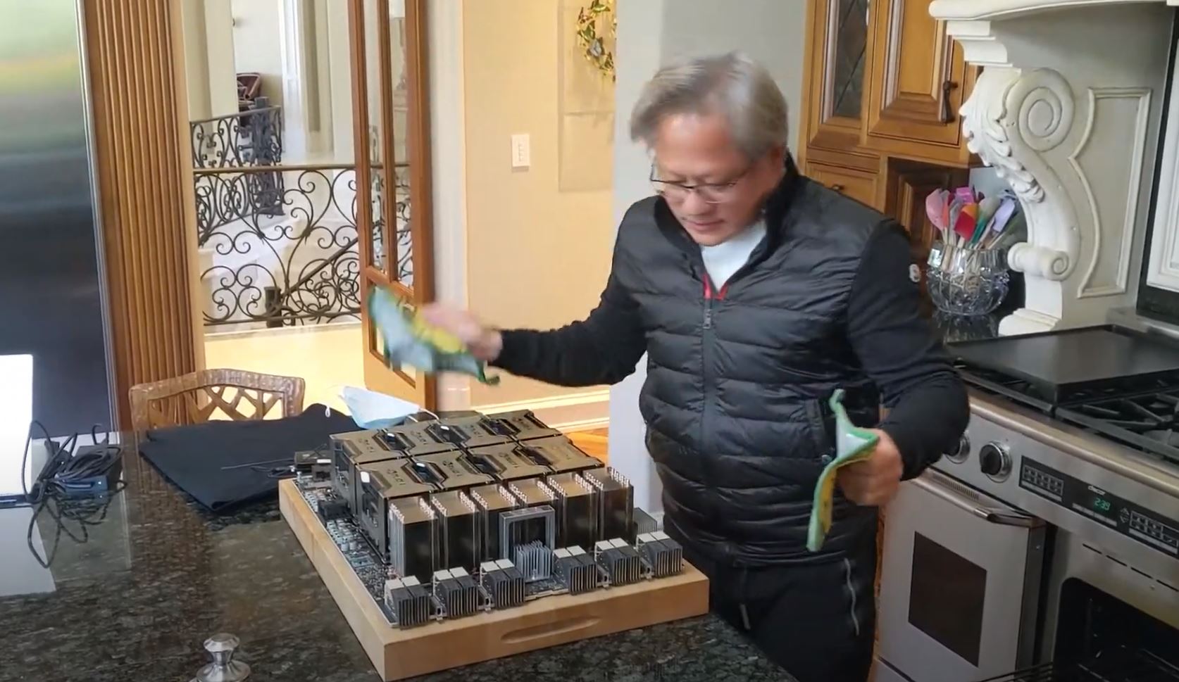
NVIDIA posted a video ahead of its GTC 2020 keynote as a teaser, but that is instructive as to what we will see from NVIDIA at the show. NVIDIA’s video was a fun nod to the shelter-in-place order that has kept shows such as GTC from happening in 2020. The company’s CEO, Jensen Huang has something cooking, and that is a new HGX-2 platform with NVIDIA Tesla A100 (GA100) GPUs. We have some details on this in light of our recent Inspur NF5488M5 Review where we just generated tens of gigabytes of images and video of our own of the Tesla V100 version of this board. Looking at differences, we can see some of the key specs emerge.
NVIDIA Tesla A100 Video by NVIDIA
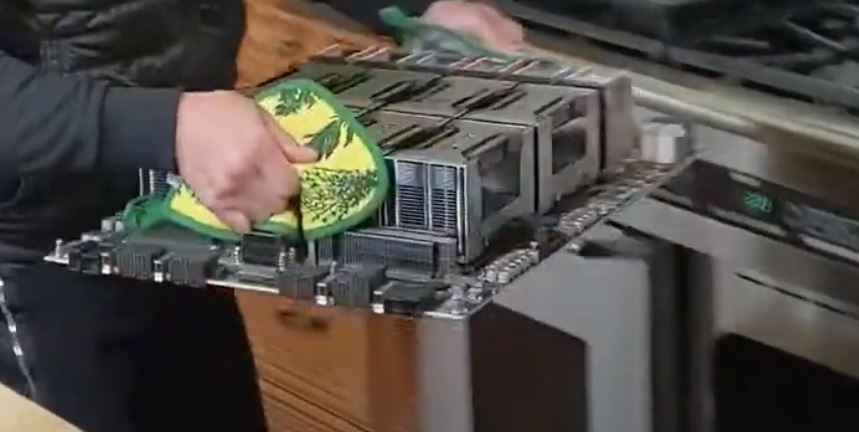
In a fun nod to the stay the least, Jensen Huang is taking a big HGX-2 board out of the oven.
At STH, we have had pictures of this assembly for some time, but wanted to respect NVIDIA’s formal launch. Since the company has now shown off the assembly from different angles, we consider it fair disclosure that we can analyze.
NVIDIA Tesla A100 Video by NVIDIA
In the video, Jensen grunts as he lifts the assembly, which is for good reason.

In our recent Tesla V100 version review, we saw that the Tesla V100 HGX-2 assembly, with sheet metal around it, weighed over 50lbs. That is an awkward weight to lift out of an oven.
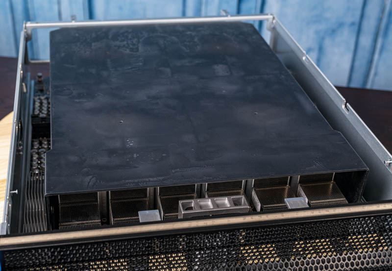
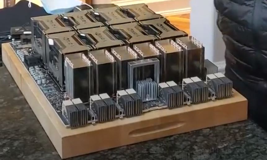
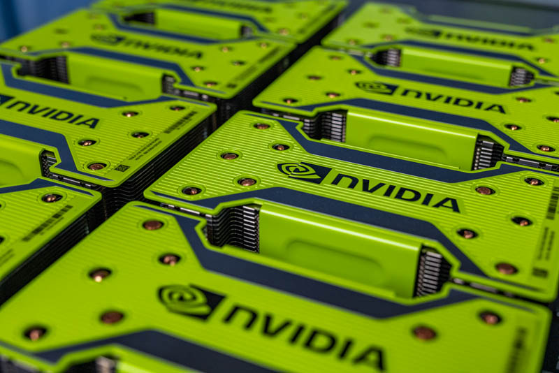
Looking at the unit, we first see the PCIe side.

Here we can see the much larger heatsinks on the PCIe and power input side of the HGX-2 baseboard.
Here are the Tesla V100 edition PCIe and power side heatsinks for comparison.
As you can see, the new NVIDIA Tesla A100 board has much more robust heatsinks on this side with more fins for more surface area. Since this is 2020 we think this is a good sign that the Tesla A100 will support PCIe Gen4 as the industry, except for Intel, has now moved to Gen4.
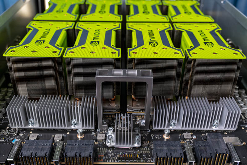
The next item we see is the NVSwitch side.
Something one will immediately notice is that the NVSwitch heatsinks are full tower coolers and much larger than the Tesla V100 version.
Here is the Tesla V100 version for comparison.
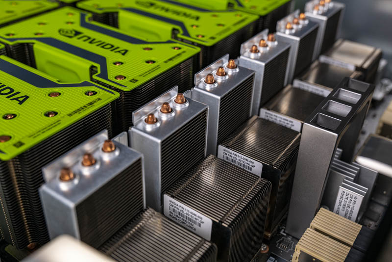
One can easily see that the new Tesla A100 version heatsinks are now full towers, not a split level design as we see on the Tesla V100 version. On the Tesla V100 version, we can see the three copper heat pipe tops on these heatsinks. On the Tesla A100 version, we can see the larger towers have a total of ten heat pipe tops.

These tower coolers are for the six NVSwitch chips on the HGX-2 baseboard. The fact that we are seeing larger coolers means that we are likely going to see an NVLink 3.0 with faster speeds. In the past, NVIDIA has looked to double NVLink bandwidth for generations, so we think that moving from 300GB/s to each SXM3 module on the Tesla V100 model is not enough for the Tesla A100 generation. Instead, with these large heatsinks, we expect that NVIDIA is going to continue its tradition offering at least twice the bandwidth with NVLink 3.0 to 600GB/s per card perhaps with NVSwitch 2.0.
On the subject of heat pipes, we will note that NVIDIA seems to have done some work on the Tesla A100 SXM3 heatsinks. We already noted in our recent review that the system was designed for “Volta-Next” GPUs that would reach 400W. So we, of course, expect the Tesla A100 GPUs will hit at least 400W, but likely more at some point as we saw with the NVIDIA DGX-2H Now with 450W Tesla V100 Modules. Here is the best we could re-construct using the angles in that video.
We can see that while the old version had the NVIDIA green shrouds over the SXM3 coolers with heatpipe ends popping through, the new “Terminator-themed” Tesla A100 coolers have a smooth finish without interruption of heat pipes.
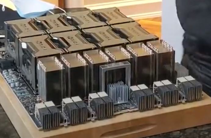
There are a few bits we can see are missing from the promotional video NVIDIA put out. A good example of that is that each SXM3 cooler module, the Tesla GA100 modules normally use the top edges of heatsinks for labeling including part numbers and serial numbers. We often also see things like that they were produced at TSMC on those labels. We do not see that with the new version shown.
Final Words
The launch of the GA100 or NVIDIA Tesla A100 is perhaps the worst kept secret in the industry. That is what happens when you have to use the part to bid supercomputer contracts and have a Tesla V100 that is nearing three years old at this point.
In terms of release date, the fact that this appears to be a PCIe Gen4 product, and the fact that NVIDIA tends to announce Tesla generations well ahead of availability, means that there is a good chance we will not see the Tesla GA100 in systems for some time. NVIDIA may do something similar with the Tesla V100 and announce the DGX system with the parts early, to capitalize on initial demand then releasing modules to other OEMs. We expect other vendors to have Tesla A100 SXM3 systems at the earliest in Q3 but likely in Q4 of 2020.
In the meantime, if you want to check out the current HGX-2 baseboard and Tesla V100 platform, here is a video overview that accompanied our review above:


This is great analysis as always STH
The idea that Intel has not moved to PCIe4 is false. Whitley is PCIe4, Rocket Lake S is PCIe4, Tiger Lake is PCIe4. Most of not all are shipping to OEMs for release later this year – which is about the time that a desktop variant of Ampere will be released.
The fact that a niche player like AMD has moved to PCIe4 is irrelevant – when they get something resembling a measurable market share, then it will matter. Their PCIe4 was nothing more than a gimmick – no way those 3rd rate Navi cards or the even worse Vega VII come anywhere near saturating an x8 PCIe3 much less a x16 PCIe4. Like their extra cores – they are a gimmick – nothing more. 1% of the user base can make use of those cores. There are very few PCIe4 cards on the market – there are NVMe on 4x PCIe4, but the mass of the market will start when Intel releases PCIe4.
Bob Whitley isn’t out until later this year right? So in the server space, no Gen4.
Everyone else: look NVIDIA has a new little video.
STH: hold my beer here’s what we can see and specs on what NVIDIA’s announcing. Oh, and in like 30 min after the video comes out.
@Bob given that AMD Rome is the current yardstick for all new supercomputer deployments AMD is the leader for my relevant fields, so I would argue that they are a bit more than just a mere “niche player”. But I agree with your point that Intel’s PCIe 4 capable CPUs will drive adoption across the wider market.
Also, why are you mixing professional products with consumer GPUs? The relevant cards in this case would be Instinct Mi50, which seem to fare fairly well in Corona (the LLNL supercomputer, not the disease).
P.S.: Does anyone know if NVIDIA supports or plans to support the OCP accelerator module (OAI-OAM) standard on current/future GPUs?
LP isn’t NVIDIA already signed on for OAM in the future? I put NVIDIA OAM in the googs and boom bam https://www.servethehome.com/facebook-ocp-accelerator-module-oam-launched/
They’ll need to support OAM if they want to sell to super 7
Great STH. I can’t wait to see your real coverage but this is way better than just reposting the vid
@Bob, show me an Intel server I can buy today that’ll handle 24x NVMe drives and 2x x16 Gen4 dual-port 100Gb NICs?
The Dell PowerEdge 7525 hit those marks a few months ago with AMD Rome CPUs. Now, the NVMe drives aren’t really Gen4 yet but we were suffering with Gen3 NICs and not enough PCIe lanes for NVMe.
Wes – they don’t have PCIe Gen4 in any of their server x86 products. That means NVIDIA would have to go EPYC for Gen4 with this or they’ll have to wait until Intel launches
@Bob
PCIe4 or faster CPU-GPU connection is really anticipated by Video processing.
PCIe3 x16 Effective CPU-GPU memory transfer speed of is around 12GB / sec, which is 12MB / millisecond.
and 4K resolution 8bit per channel RGB image is 3840 x 2160 x 3 = 25MB per frame.
So precious 2 millisecond is needed just to transfer 1 frame image from CPU to GPU.
Now 4K deep color(6 bytes per pixel) 50MB/frame 8K 100MB/frame or even 8K deep color 200MB/frame is coming.
8K 120Hz deep color video is impossible to display in real time speed using PCIe3 x16 link.
Comments are closed.