
Intel rolled out a number of new announcements on the IPU side. For those unaware, Intel is focused on not adopting the industry “DPU” term instead opting for the “IPU” term that coincidentally starts with “I” like “Intel” and is confusingly similar to the Graphcore IPU. We recently looked at how the company’s current offerings Intel IPU is an Exotic Answer to the Industry DPU. There, the company mostly showed off FPGA solutions we dubbed “exotic” in the STH NIC Continuum. Now, Intel has more exotic IPUs along with its first DPU ASIC. It also seems as though Intel is ceding the DPU market to Arm.
Background: The STH NIC Continuum
A few weeks ago we published the STH NIC Continuum Framework to help our readers classify different solutions such as offload NICs, SmartNICs, DPUs, and exotic offerings. Here is the video for that:
We have spoken to many industry vendors and most have adopted this framework over the past year since our What is a DPU A Data Processing Unit Quick Primer piece. DPU has become the industry term for a specific class of device as we can see on the STH NIC Continuum.
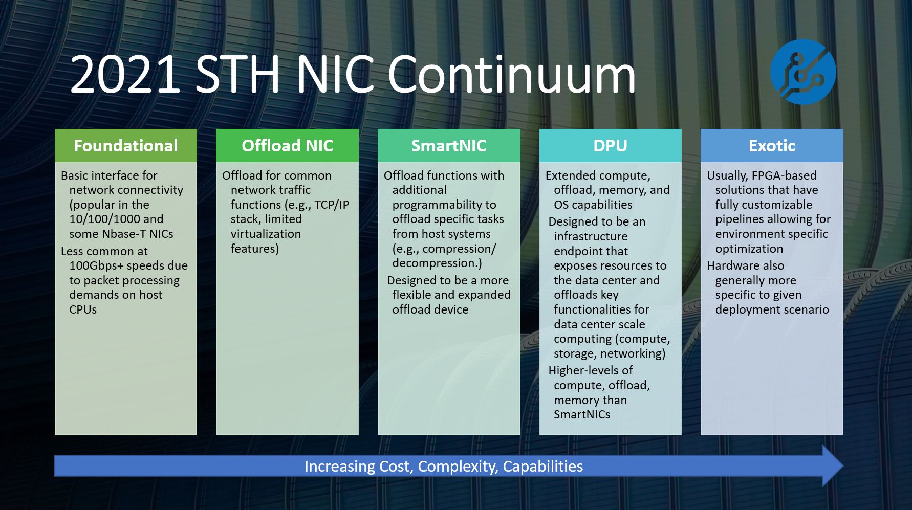
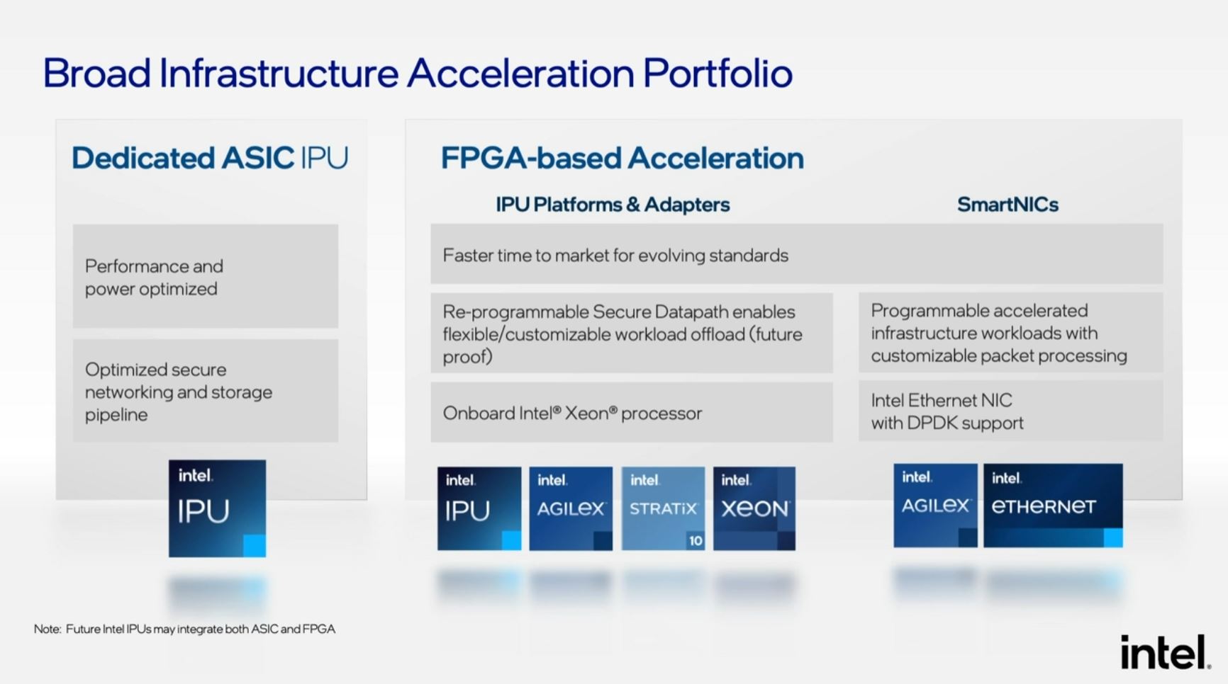
Intel is using IPU as its term, and perhaps for a different reason than our classification system. Intel has not only the Dedicated ASIC IPU but also exotic FPGA-based platforms, SmartNICs, and offload NICs (Intel puts its E810 NIC as an example in SmartNIC but as part of the STH NIC Continuum we would put this as an offload NIC.) With Intel’s enormous portfolio that spans all five categories of the Continuum, perhaps the key is that Intel needs to brand a portfolio beyond a single solution.
With nomenclature aside, Intel has a number of new products that are exciting advancements across its Intel Infrastructure Processing Unit portfolio. Let us get to those.
Intel’s IPU Push
If you have seen our content on DPUs then this will be familiar. Still, Intel reiterated the advantages of DPUs.
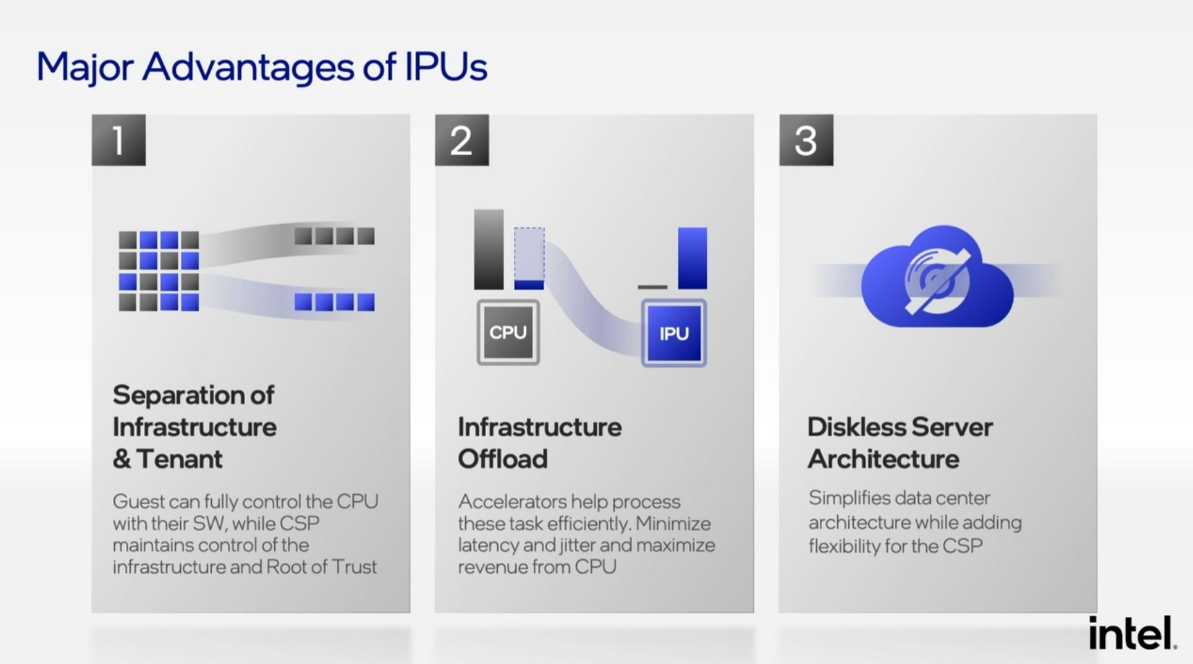
The first point really focuses on separating the infrastructure and application layer. This is the same concept we have heard from other companies such as NVIDIA, Marvell, Pensando, and others. Running hypervisor plus storage, networking, encryption and more on a DPU in a manner more similar to how AWS pioneered with Nitro is the way that the industry is moving.
A key benefit is that by offloading tasks such as the networking stack, storage stack, machine management, and crypto/ compression tasks from the CPU, one can free up valuable CPU cores. Cloud providers today that do not use DPUs cannot sell the entire CPU capacity in virtualized hosts because of all of these overheads. If one has two 40 core CPUs in a server and needs to use four of those cores to run networking and storage then 5% of the server’s resources are not available to sell. As infrastructure providers add more services such as firewall and packet processing capabilities, the pressure on the CPU becomes greater meaning the offload becomes more valuable.
One we generally discuss in the first two, but that is useful for getting to an odd number of benefits is the ability to run “diskless” servers. DPUs can access network cluster storage or remote storage and then present a NVMe device to the server that effectively looks to the server like it is a local device. As a result, storage can be moved outside of the server allowing for higher utilization and greater deployment flexibility.
With that, let us get to the new products, starting with some of the more exotic IPUs.
Intel N6000 Arrow Creek
When Intel launched the Intel PAC N3000 it was a big deal. This was an easy way to start adding FPGA-based network function acceleration directly into servers. We even looked at a Supermicro SYS-1019P-FHN2T with Intel PAC N3000 in our hands-on. What Intel found was that the FPGA with network ports on a standard PCIe card sold by OEMs ended up being popular with developers (and is something Xilinx Alveo is designed to leverage.) Now, Intel has a next-generation, the Intel N6000 Acceleration Development Platform codenamed Arrow Creek.
Arrow Creek is a big upgrade. There are dual QSFP56 connectors for dual 100GbE along with PCIe Gen4 support (necessary for that speed.) There is also a clocking tool with antennas. In many industries, such as financial services, tight timing requirements exist to ensure the accuracy of synchronized logging. That is a small but important feature if you work in those industries.
The FPGA is now an Agilex generation and we get 17GB of memory. 1GB is for the Arm CPU in the Agilex. 16GB is for the programmable logic function of the card. One can see that we also have a Max 10 FPGA and an Intel Ethernet controller. The Ethernet controller is the Intel E810. The key here is that this is more of a programmable exotic NIC rather than a basic NIC or a DPU.
Intel Oak Springs Canyon
The Intel Oak Springs Canyon is new, but it is also something we have seen before. We covered this in our Continuum piece, but Intel has had the Inventec SmartNIC C5020X platform and similar options for some time. The basic concept is combining a FPGA with a Xeon D CPU to give x86 compute alongside FPGA flexibility on a single NIC.
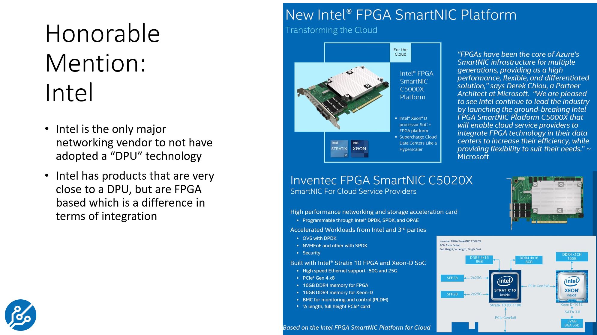
The new Intel Oak Springs Canyon seems to take this concept to the next level. It replaces the Stratix 10 FPGA with an Agilex part yet both the Xeon D and FPGA still get 16GB of memory each.
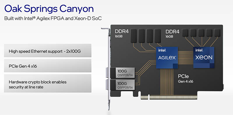
Since this new generation is a PCIe Gen4 part, we asked Intel if this was using Ice Lake D or another part. Ice Lake D was mentioned at the Intel Xeon Ice Lake Launch but products are not generally available yet. Intel told us it is not disclosing this at this time.
Still, it seems like Intel has a customer or customers that like this FPGA + Xeon D exotic solution enough that we are seeing another generation of this setup.
Intel Mount Evans DPU IPU
Intel finally has a new DPU to compete with the NVIDIA BlueField-3 and Marvell Octeon series. The new DPU IPU is called the Intel Mount Evans. This is a huge deal. Here is the highlight with the top one being that this DPU IPU was designed with a large cloud provider.
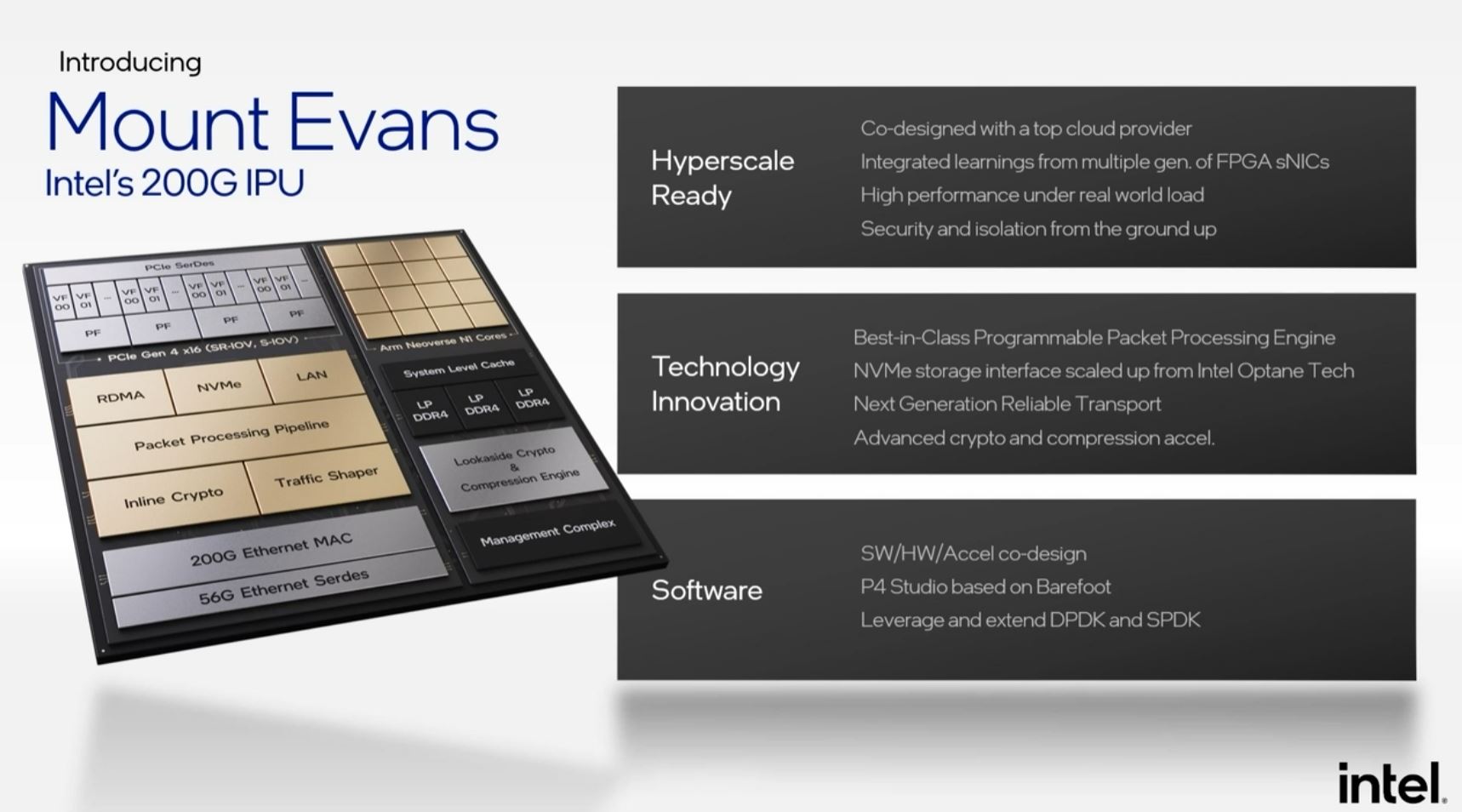
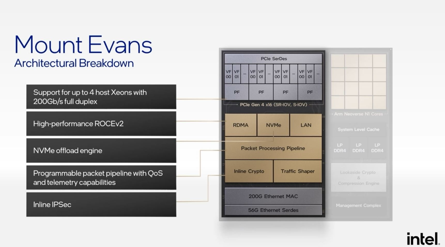
Effectively, the 200G generation Mount Evans DPU IPU has two hemispheres. One side is the networking subsystem while the other is the compute complex.
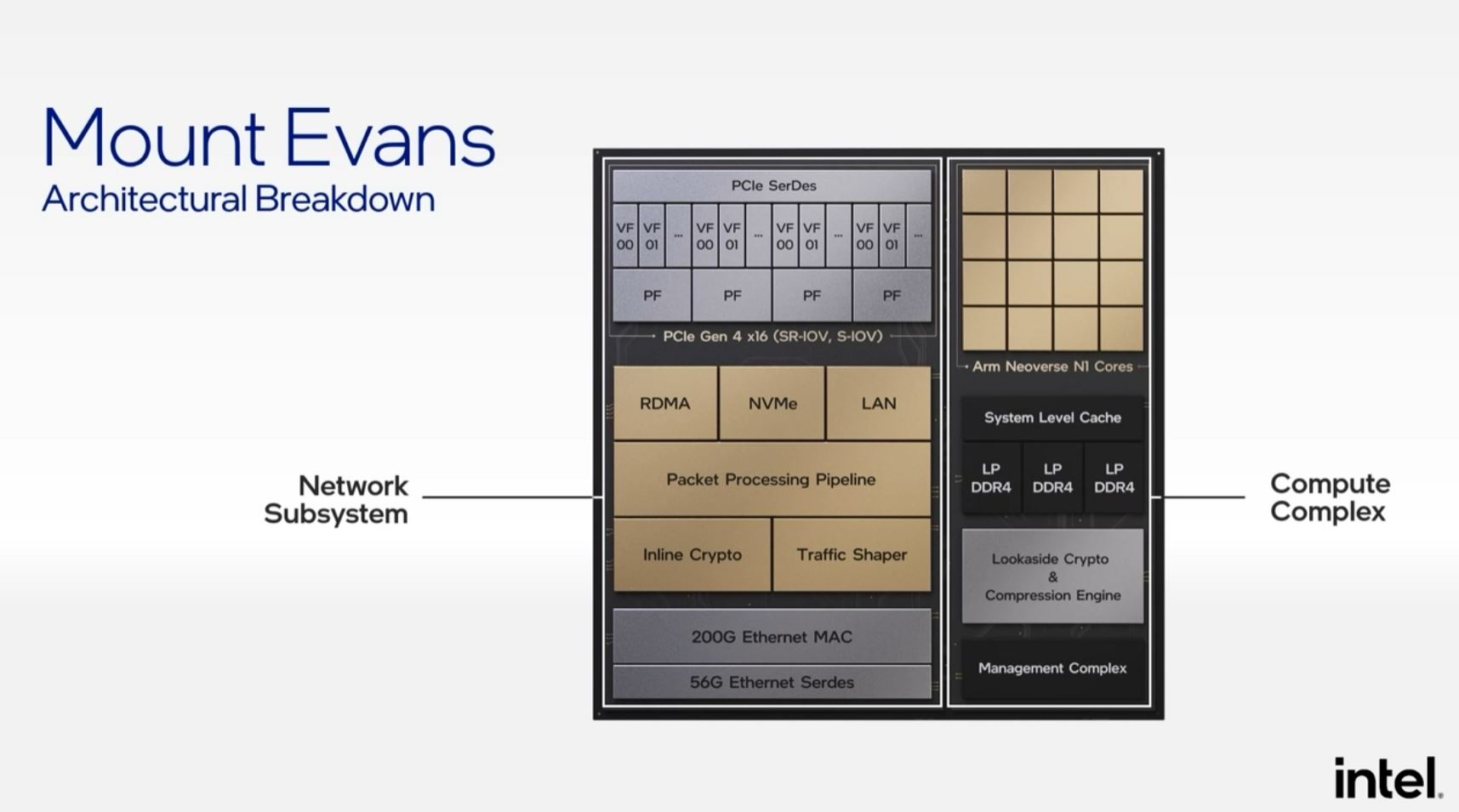
On the networking side, Intel has the PCIe capability to use this as a multi-host adapter platform connecting up to four CPUs over PCIe. Multi-host adapters are a way for large cloud providers to run networks more efficiently. Here we have crypto accelerators and features for NVMe/ ROCEv2. The packet processing pipeline takes P4 learnings from Intel’s Barefoot acquisition. For a company like Pensando with its Distributed Services Architecture, Intel getting into the market with a P4 capable DPU should be a scary proposition.
On the CPU complex side, we have “up to 16 Arm Neoverse N1 cores.” One can think of these Neoverse N1 cores as similar to AWS Graviton2/ Ampere Altra generation cores. This is quite interesting since at Intel Architecture Day 2021 Intel discussed its Gracemont cores which one would think could be an alternative here, but Intel instead is going with Arm. We may be seeing Intel cede the DPU market to Arm. The company has the exotic options with Xeon D, and companies like Fungible use MIPS (one wonders for how long) but otherwise, this is a market Arm is dominating. Further, since this is a product Intel is touting as being designed with cloud provider input, it seems as though that cloud provider wanted Arm not x86. Intel uses Arm extensively in areas such as its FPGAs as well as other accelerators, but given that even Intel is using Arm here, it seems as though the writing is on the wall for the DPU market.
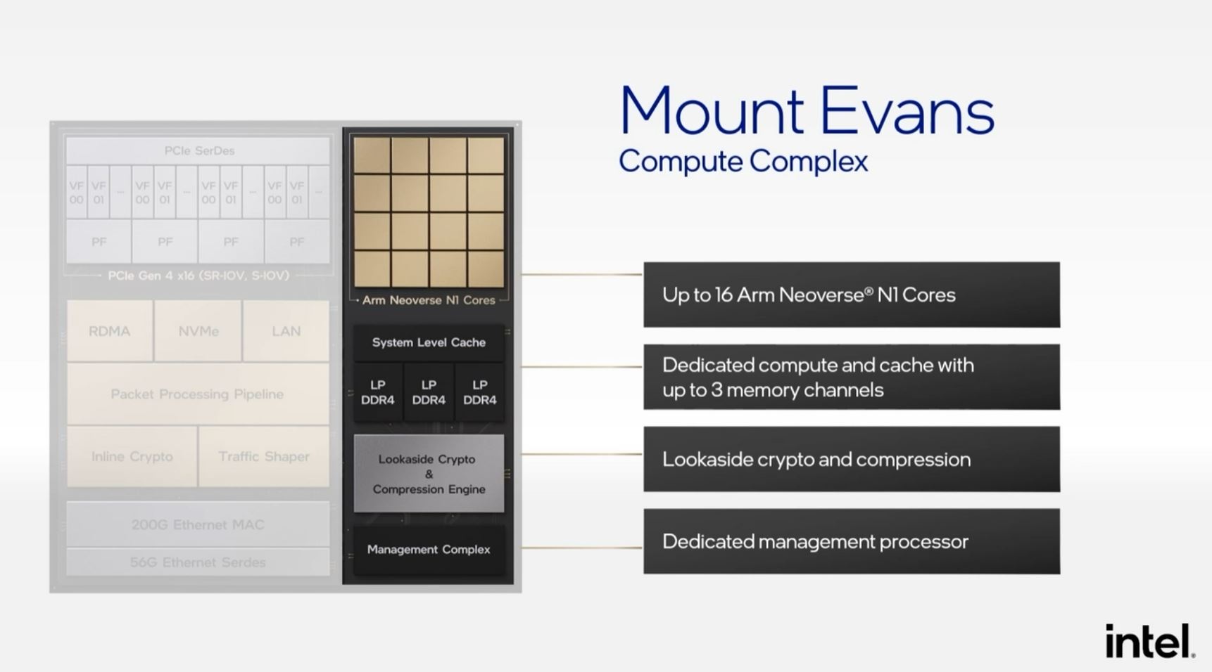
Rounding out features that qualify this as a DPU we also have LPDDR4 memory channels and a management complex along with the accelerators. Assuming this is placed on cards with storage for the OS and NIC ports, then this is Intel’s first product we would consider a DPU.
As a quick aside, sixteen Arm Neoverse N1 is a lot. As we have been working with the Mellanox NVIDIA BlueField-2 DPU in the lab, the CPU of the NVIDIA solution leaves a lot to be desired. Sixteen Neoverse N1 cores should help that considerably. We will quickly note that Marvell Octeon 10 400Gbps PCIe Gen5 DPUs will utilize newer Arm Neoverse N2 cores and at much higher core counts (even the development platform in Q4 2021 will be 24x Neoverse N2 cores) and have higher levels of acceleration.
There is one glaring omission from the Intel Mount Evans platform. The NVIDIA BlueField-2 DPU was conceived prior to the NVIDIA-Mellanox acquisition. Every time I get the opportunity to ask Jensen Huang, NVIDIA’s CEO, about the future of BlueField, it involves AI acceleration. Marvell is building in AI inference as this is seen as a key capability. Intel seems to have a product that it is disclosing in the second half of 2021 but that does not include AI acceleration blocks.
That stood out as different from most of the industry and where we have heard others in the industry say that this is what will be required in the future.
Still, it is very cool that we now have something from Intel that could be considered a DPU even if we did not get shipping timelines.
Final Words
Overall, these are some great announcements from Intel. Moving Agilex into more of the company’s exotic NIC portfolio gives new levels of technology to developers and its customers. Further, even though Mount Evans has some intriguing inclusions and omissions, adding a DPU to Intel’s IPU portfolio is a great step. With Intel, NVIDIA, and Marvell pushing heavily in the market, we need to see new offerings from Broadcom, Xilinx(/AMD), and the host of startups to compete with these new solutions from the large infrastructure players.
Very cool by Intel!


I’d be fascinated to know whether the ‘top cloud provider’, and their presumable desire to be able to diversify vendors if needed, or whether Intel’s own comparisons and engineering constraints led them to go with the ARM cores on the Mount Evans part.
It’s a bit of a surprise because Intel certainly has server-grade Atom cores on hand (often priced in a way that suggests they dislike you personally for not buying Xeons; but that’s a problem that can be solved on paper rather than with intensive engineering effort) and those already have ubiquitous software support as well as QAT and similar offload features.
Given that Intel presumably prefers to use an internal part rather than giving ARM a PR win(and some licensing fees) they must have had some compelling reason.
The using of the ARM N1 cores has maybe something to do with timing and risk control. The rumour is that the Mount Evans design cycle started about a year ago and using the new Gracemont core in the design at that moment should be a great timing risk (as the prototype chips had to be ready in April, to convince the ‘top cloud provider’). I see Mount Evans more as a release1 design that will be rather quickly followed by a next one. The most important question here is if Mount Evans is a chiplet design, if so design iterations will follow quickly, even with x86 or ARM versions at the same time…. Maybe we will hear more design details at Hot Chips 2021 that has a timeslot (on Monday) for a Intel IPU presentation :-)
fuzzy fungus: Agreed.
Its tragic that Intel purposefully handicapped Atom development all these years else they might be in a better place to position them as an alternative, but the market has already decided on ARM for these dedicated tasks it seems.
Comments are closed.