AMD EPYC 7003 SoC Features
Although a simplistic view, one way to look at how AMD operates is that it has its Zen microarchitectures, but then it has other teams that package those Zen cores into sellable units. In this article, we are looking at the EPYC 7003 series, but other examples are the workstation Ryzen Threadripper PRO, the desktop Ryzen 5000 series, and even with GPU IP for the 1L corporate desktop PC segment we saw in our Lenovo ThinkCentre M75q Gen2 Tiny Review. In this case, let us look at how it becomes the Milan SoC.
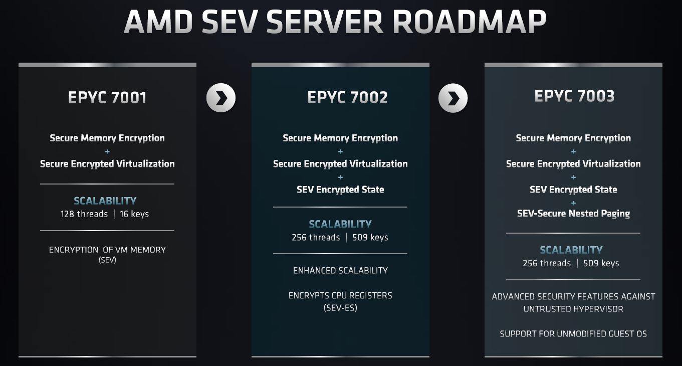
This slide probably had a different intent, but this is a great opportunity to point out the EPYC 7001 to EPYC 7002 versus the EPYC 7002 to EPYC 7003 transition. Here we can see the latest transition is relatively mundane with many of the platform features largely the same. That informs what we should expect looking at the SoC construction.
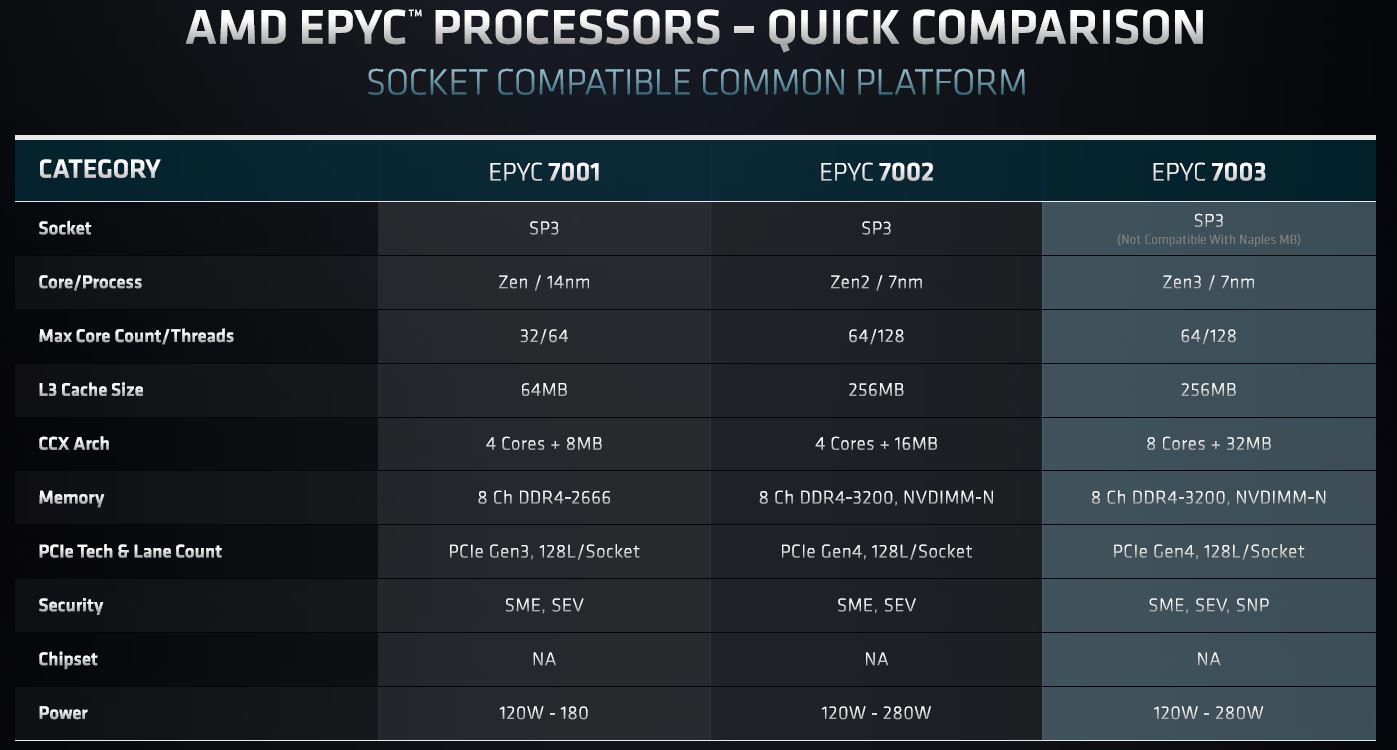
Here is the high-level overview with the changes highlighted. For those wondering about the “162 PCIe lanes”, that is the 160x PCIe lane 2P configuration we covered in the Dell and AMD Showcase Future of Servers 160 PCIe Lane Design piece plus the two WAFL PCIe Gen2 lanes for features such as Baseboard Management Controller connectivity.
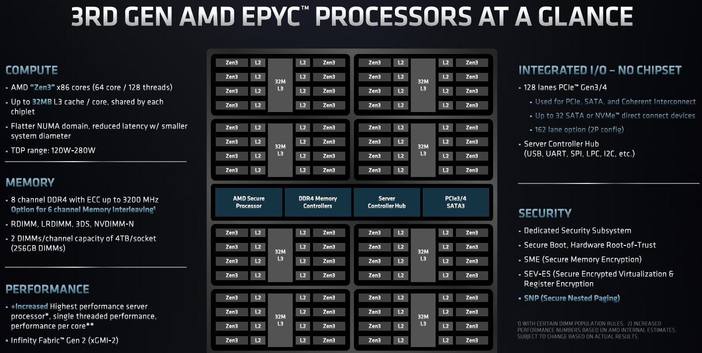
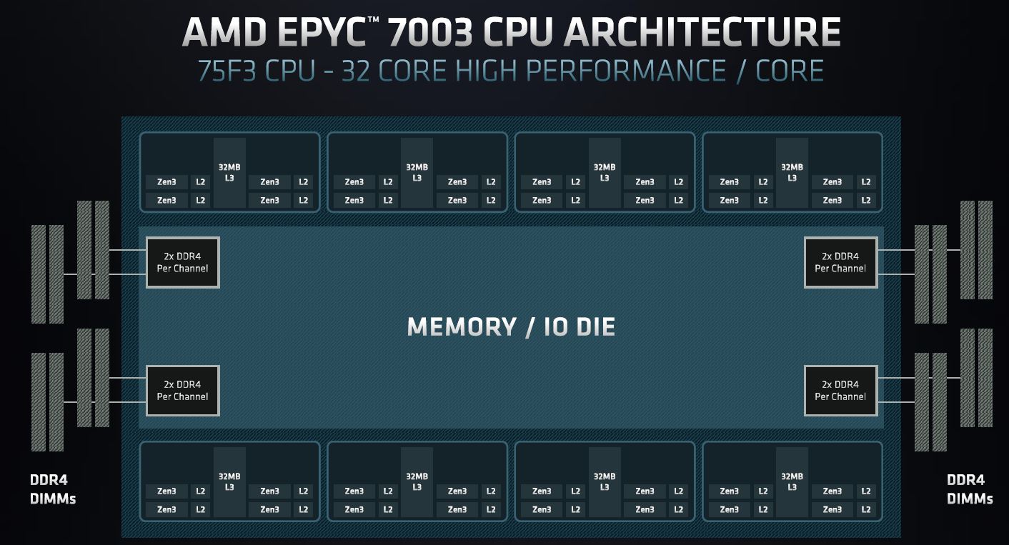
In terms of architecture, AMD is going to focus on a clear change its cache and CCX topology. In AMD nomenclature you can think of CCX as a cluster of cores that has access to a L3 cache. A CCD is a die that has the x86 cores and L3 cache. The I/O die is labeled “Memory/ IO die” below and that ties all of the chiplets together while providing external I/O.
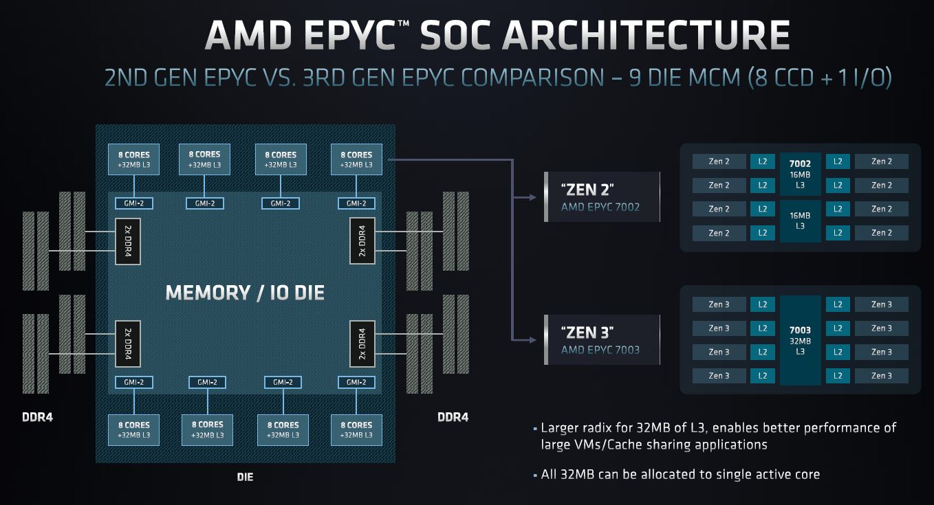
The big change in this generation is that a CCD previously had two sets of up to four cores each with 16MB of L3 cache. While these segments shared the same die, there was a penalty when crossing the CCX boundary even on the same die. In “Rome” this meant we had up to 8 cores and 32MB of L3 cache, but that was effectively split due to this CCX division. In Zen 3, AMD unifies all of these on-CCD resources. As a result, the penalty for going back through the I/O die is still present, but access domains for L3 caches have moved from 4 cores to 8 cores. Also, 32MB is a lot of cache for eight cores so one gets a more efficient radix and use of resources.
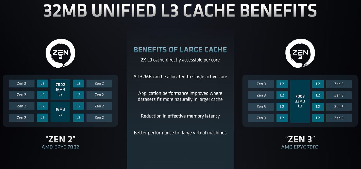
This setup also means we get some interesting new topologies. The AMD EPYC 75F3 that we will have benchmarks of later has four cores per CCD, but also four cores per CCX with 32MB of L3 cache for a total of 8MB/ core. Current Cascade Lake Xeon generations L2+L3 cache total capacity is closer to 1/3 of that.
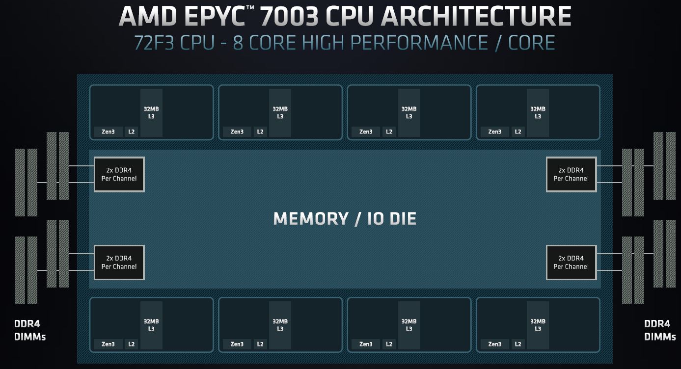
Where things get borderline crazy is with the EPYC 72F3. One may have seen we have the Xeon Platinum 8356H which is Intel’s 8-core Cooper Lake part. AMD’s part has 32MB of L3 cache per core and is an 8 core/ 256MB L3 cache chip. In the EPYC 7002 generation, one would have only had half as much L3 cache per core.
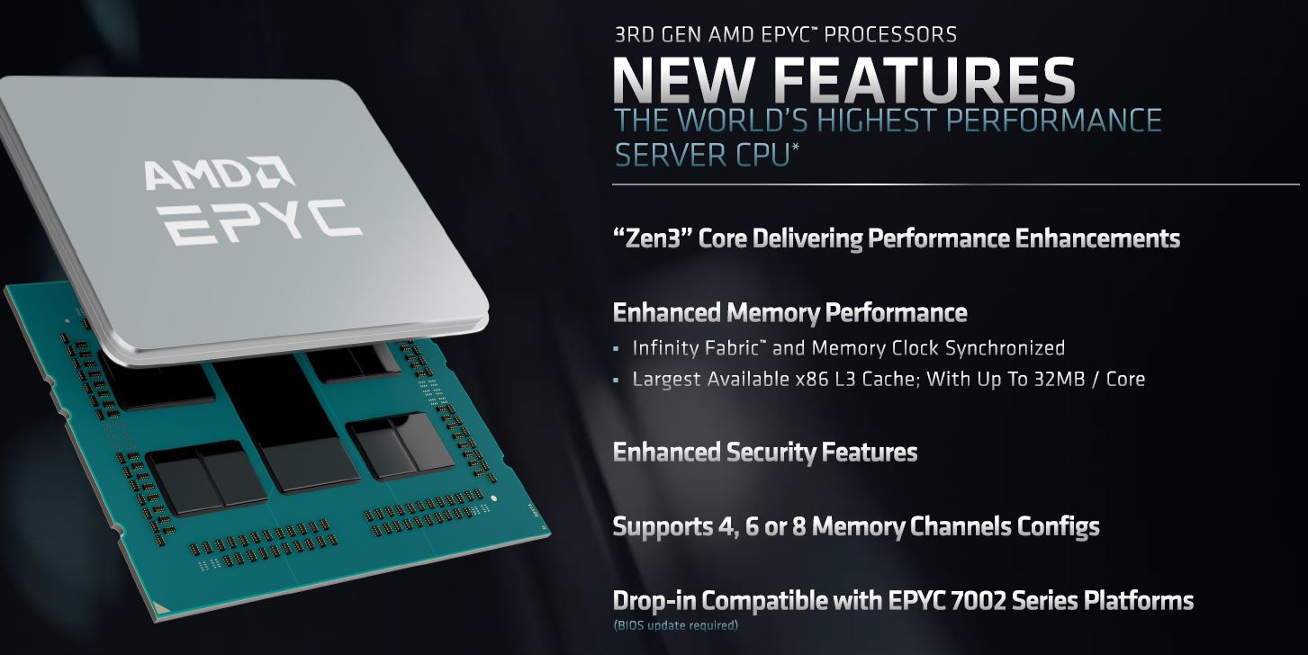
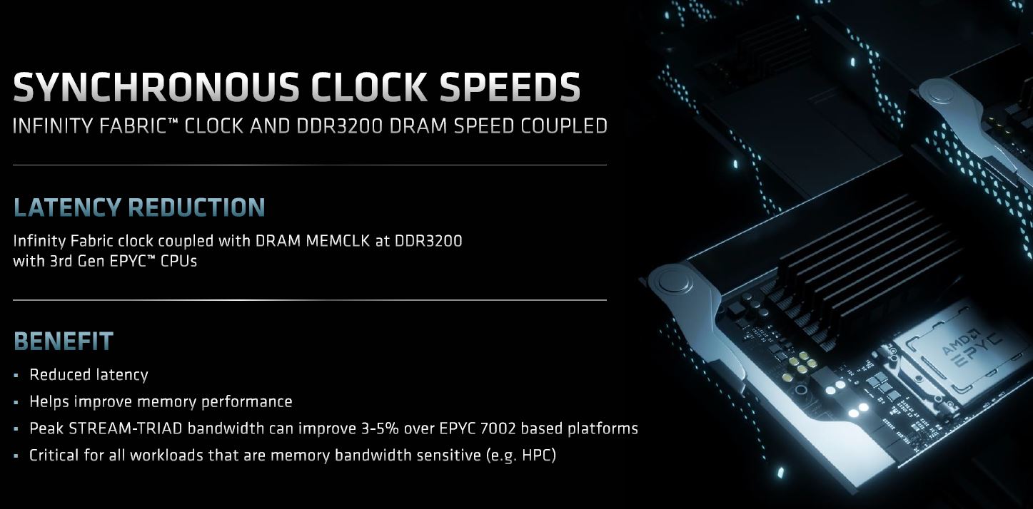
AMD also has synchronized the Infinity Fabric and memory clock meaning that there is lower latency from not having to switch clocks.
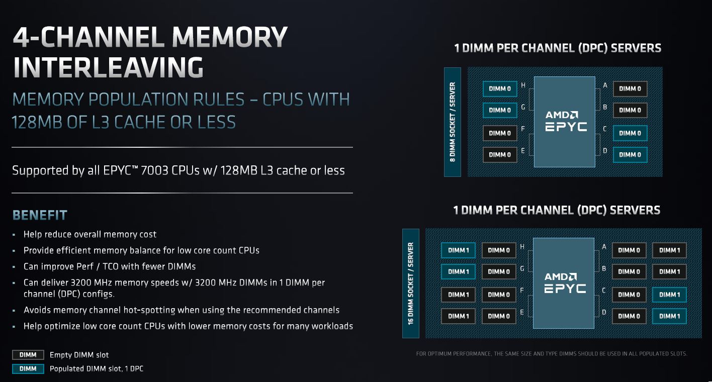
We typically test servers in one DIMM per channel or 1DPC mode. However, there are many segments that do not want that much memory because they are very cost-sensitive. AMD has had a 4-channel memory mode where it optimizes for these lower-memory populations. The context around this is that the Xeon E5 series for years had 4-channel memory so there are many customers who are being begrudgingly moved from using 4x8GB DIMMs to 4x 16GB DIMMs due to increasing memory module capacities. These are buyers who do not want to have 8x 16GB DIMMs. While to those reading this article to learn about performance this may seem crazy, this is simply a cost-driven market dynamic.
Then we get to perhaps the most interesting one, the 6-channel memory mode. As with the 28/56 core SKUs, this is clearly meant to target buyers coming from Skylake Xeons. Effectively AMD can offer someone using 6x 16GB with a Xeon Platinum 8180 (I am not sure if there is anyone out there doing this) a path to have a 28 core CPU with 6 memory channels populated.
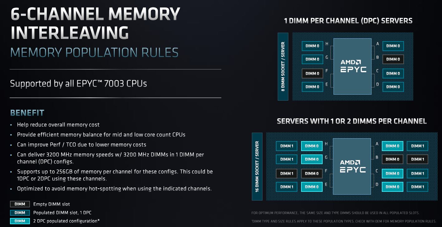
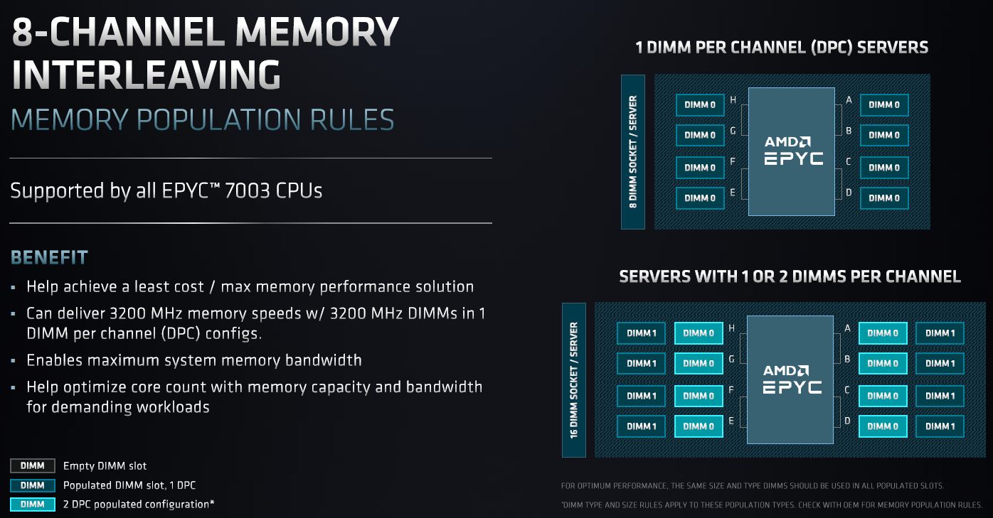
In a “perfect” world everyone would just do an 8-channel memory population, but that is not the case. Hence why we have a 4 and 6 channel memory population option.
Those are the big SoC features, except for security which we wanted to discuss separately.
AMD EPYC 7003 Security Features
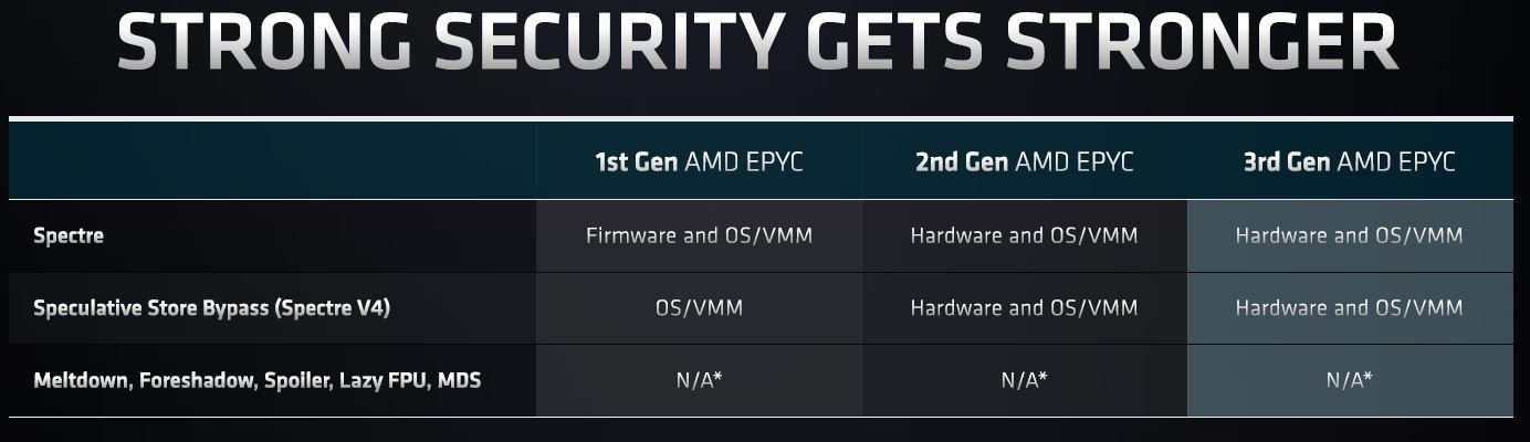
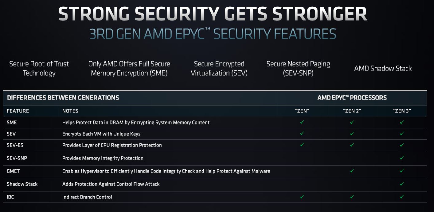
AMD has a number of security features. One of them is that it has speculative execution mitigations. This chart may not make it look like there are advancements, but we were told AMD did make progress.
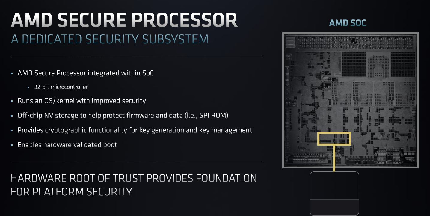
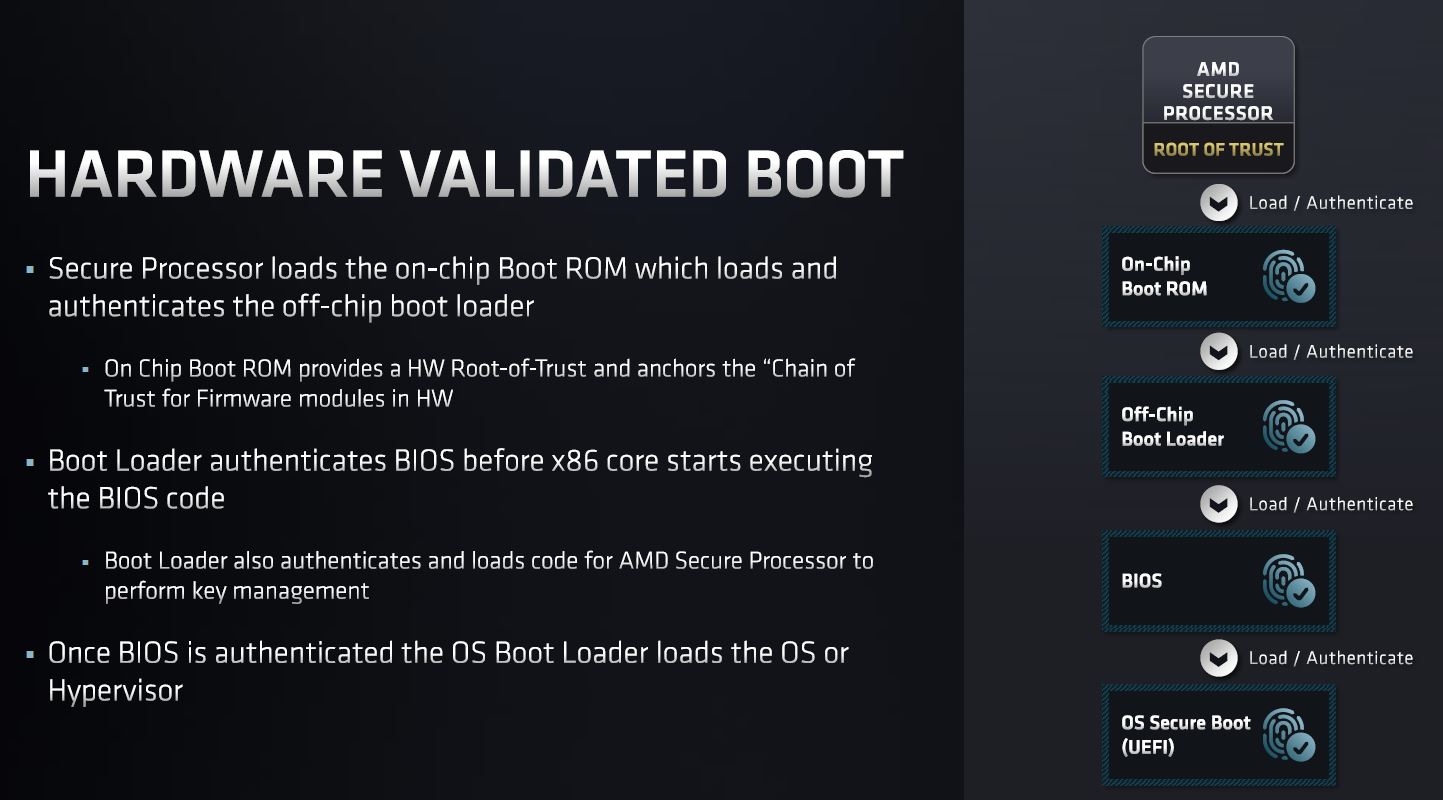
Part of AMD’s value proposition is that it has an Arm-based processor on the SoC itself. This is the AMD Security Processor and handles a lot of work such as key management, hardware root of trust, and hardware validated boot.
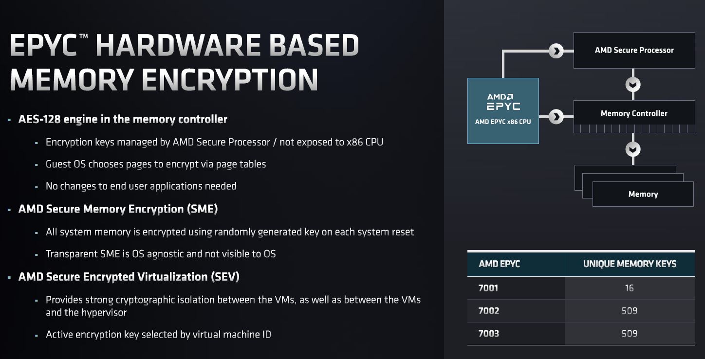
Part of AMD’s secure memory encryption and virtualization offering is set to enable the concept of confidential computing where the cloud provider does not have access to your instance. AMD had a big win when Google Cloud Confidential Computing adopted AMD EPYC 7002 Rome for its offering. Intel will be moving into this space, but AMD has deployments so expanding capabilities is important.
AMD has hardware validated boot from the security processor. As part of this AMD PSB can be used to blow field-programmable fuses and lock an EPYC CPU to a vendor’s platform (Dell does this as an example.)
AMD has memory encryption with the same memory key limit as the AMD EPYC 7002 “Rome” generation.
As one can see, we now get SEV secure nested paging and the ability to run unmodified guest OSes securely.
To some of our readers, these are going to be the most exciting features. To others, it is onto the numbers so let us get to the performance.
Next, we are going to get into the performance aspects of the new series.


Any reason why the 72F3 has such conservative clock speeds?
The 7443P looks as if it will become STH subscriber favorite. Testing those is hopefully prime objective :)? Speed, per core pricing, core count – there this CPU shines.
What are you trying to say with: “This is still a niche segment as consolidating 2x 2P to 1x 2P is often less attractive than 2x 2P to 1x 2P” ?
Have you heard co.s are actually thinking of EPYC for virtualization not just HPC? I’m seeing these more as HPC chips
I’d like to send appreciation for your lack of brevity. This is a great mix of architecture, performance but also market impact.
The 28 and 56 core CPUs are because of the 8-core CCXs allowing better harvesting of dies with only one dead core. Previously, you couldn’t have a 7-core die because then you would have an asymmetric CPU with one 4-core CCX and one 3-core CCX. You would have to disable 2 cores to keep the CCXs symmetric. Now with the 8-core CCXs you can disable one core per die and use the 7-core dies to make 28-core and 56-core CPUs.
CCD count per CPU may be: 2/4/8
Core count per CCD may be: 1/2/3/4/5/6/7/8
So in theory these core counts per CPU are possible: 2/4/6/8/10/12/14/16/20/24/28/32/40/48/56/64
I’m wondering if we’re going to see new Epyc Embedded solutions as well, these seem to be getting long in the tooth much like the Xeon-D.
Is there any difference between 7V13 and 7763?
Comments are closed.