What Changes with AMD EPYC “Rome”
With AMD EPYC “Rome”, there are two I/O die with x86 cores that hang off the I/O die. When we look externally, AMD has a set number of pins that need to carry data to and from the socket. That includes pins for eight memory channels along with eight x16 links. We are going to leave the memory channels alone, and discuss the x16 links.
With AMD EPYC 7002 or “Rome” already has PCIe Gen4 support announced, while the 2nd Gen Intel Xeon Scalable CPUs still use 14nm and Intel’s PCIe Gen3 IP. In a single socket, that means that AMD EPYC Rome will have 128 PCIe lanes using eight x16 links for PCIe. We expect AMD will use the Rome generation to add another PCIe lane, making 129 PCIe lanes total, and we are going to discuss that in our “Bonus Lanes” section later.
PCIe Gen4 is significant. AMD has to upgrade their SerDes to accommodate essentially twice the bandwidth of PCIe Gen4 along with faster chip to chip IF. Using the rough model that Infinity Fabric on the first generation was using the Gen3 speed, the AMD EPYC Rome Infinity Fabric links are set to double in speed.
Doubling speed means that AMD’s aggregate socket-to-socket I/O die to I/O die bandwidth will increase much faster than we have seen Intel move from QPI and UPI generations. With the 2nd Gen Intel Xeon Scalable chips, Intel is still using 10.4GT/s UPI. Quad socket Intel Xeon Scalable systems have one UPI link between sockets. Dual socket systems will usually have two links but may have three on higher-end PCB systems. AMD’s aggregate socket-to-socket bandwidth is set to double taking what was a closer cross-socket story, to a lopsided benefit.
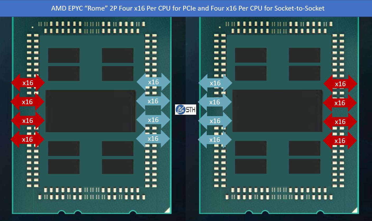
Having so much bandwidth available raises questions. Does one need 64 (4×16) lanes between the two sockets? Since AMD uses a flexible interconnect in their PCIe and Infinity Fabric designs, and because the SP3 socket is designed for 128 of these lanes, AMD and its platform partners have an option: they can use fewer 16 lane sets for socket-to-socket bandwidth.
For those that will want PCIe Gen4, we have had it confirmed since before Rome was officially announced that many platforms will see new generations. PCB quality used was fine for Gen3, but Gen4 needs better PCB to ensure that the communication channels stay clean. For smaller single socket compact systems, some vendors think they will not need a PCB re-spin to support PCIe Gen4. For larger systems exposing large numbers of PCIe lanes, as we have discussed previously, they will require a Gen4 re-spin.
With new PCB and a virtual superhighway of socket-to-socket bandwidth, some systems designers are looking at using x16 links for additional PCIe Gen4 connectivity versus socket to socket Infinity Fabric links. Instead of using four x16 links on each CPU for socket-to-socket, vendors are looking at Rome re-spins as opportunities to use one x16 link on each CPU as extra PCIe Gen4. Using five of the x16 lane sets on each CPU for PCIe gives 160 total instead of 128 using four-lane sets.
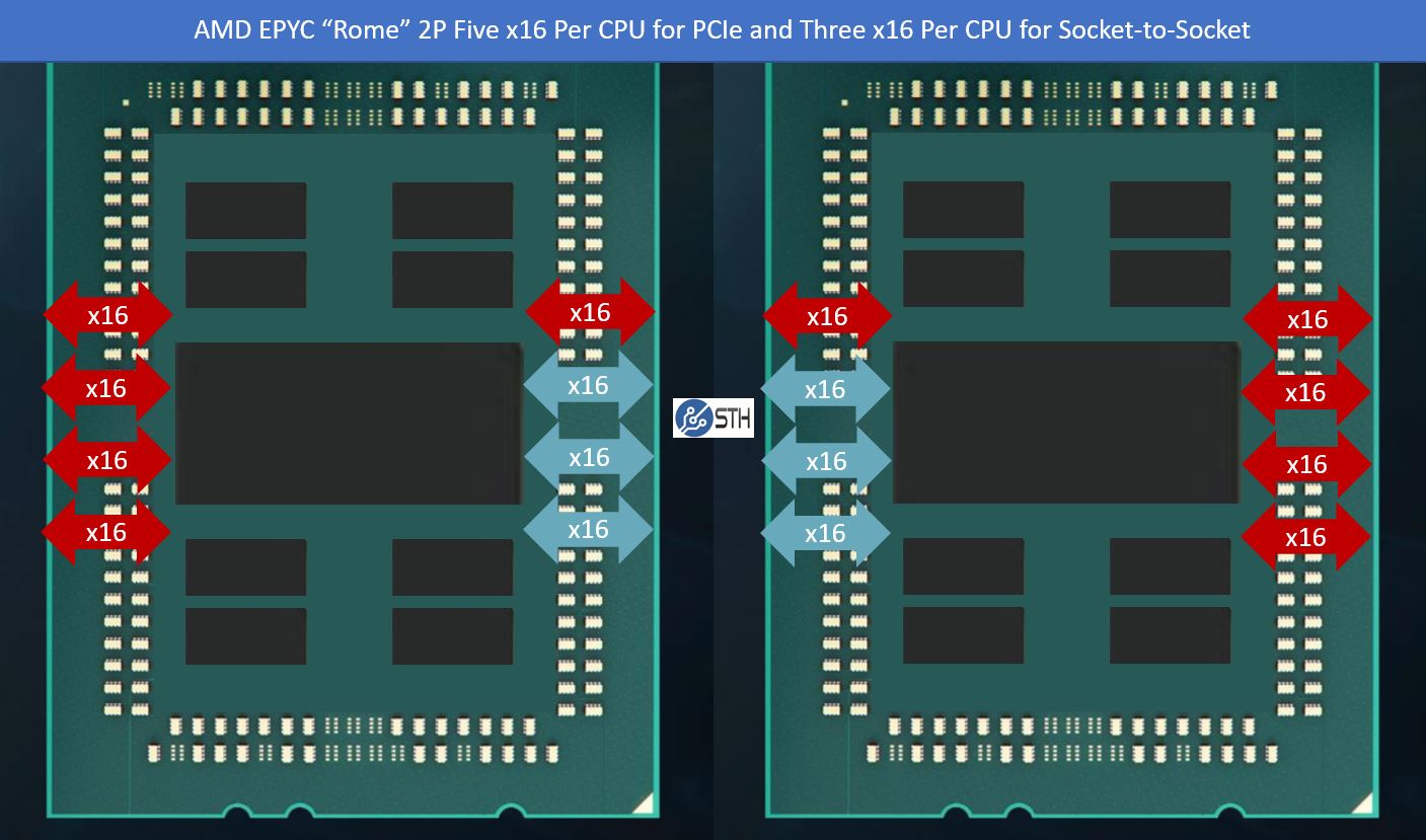
Some systems designers may elect three x16 socket-to-socket links rather than four, instead choosing to maximize PCIe Gen4 lanes at 160. That will decrease socket-to-socket bandwidth which is not necessarily desirable. It also does not fit well with some of how larger systems vendors look at systems. For more niche players, and those willing to accept this trade-off, this is a possible way to differentiate and create very cool platforms for applications like GPU compute, NVMe storage, traditional SAS storage, and Xilinx CCIX FPGAs.
In theory, using two x16 lane sets would allow for similar socket-to-socket bandwidth as current “Naples” chips at twice the speed and half the lanes. From what we hear, and given the additional system girth we can see with Rome, a two x16 lane for Infinity Fabric topology will not be officially supported. If it was supported by AMD and its partners, that would allow similar socket-to-socket bandwidth as today. Stepping down to fewer links cross-socket would require additional validation resources, and given how much compute, RAM, and PCIe the system will support, it is a trade-off AMD is not expected to invest in.
Update 05-April-2019: We have not heard of an OEM supporting 2x inter-socket links with 2×6 x16 (192) PCIe lane configurations yet, even though it would be good for their AMD’s GPU division.
That still does not solve a constraint found on “Naples” that Intel does not face: the lack of a PCH. Without a PCH, on the AMD EPYC 7001 series, one loses many lanes due to lower-speed I/O such as the BMC. This lower-speed I/O is one of the reasons we do not see systems with 128x PCIe Gen3 lanes exposed today. AMD is aware of this and has a plan to fix it.
WAFL Bonus PCIe Lane(s)
Unlike Intel’s PCH, AMD’s chips are designed to have all I/O on package. When looking at 1st and 2nd Gen Intel Xeon Scalable systems versus AMD EPYC, one has to remember that Intel systems include a Lewisburg PCH that uses power and adds cost.
AMD had a goal of using flexible I/O and its Server Controller Hub (SCH) to remove the need for the PCH.
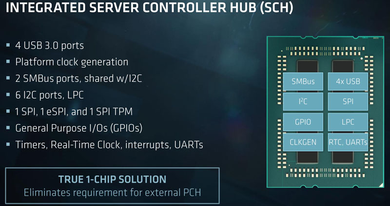
To address the extra I/O needs of adding lower-speed devices like a server’s BMC, AMD is readying an extra lane per CPU. From what we understand, these are not meant for high-end devices. Instead, these are meant to relieve the main x16 lane blocks from being used by lower-speed devices. A common one is the server’s BMC.
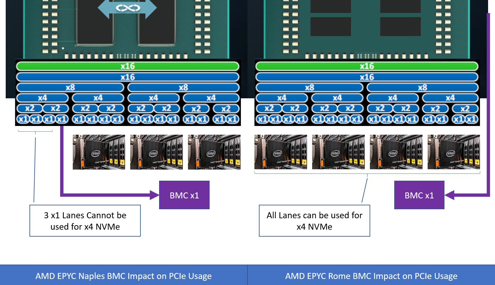
As we have worked with dozens of AMD EPYC platforms and published many reviews, a common question is why the platforms do not expose 128x PCIe lanes to the motherboard or server in the AMD EPYC 7001 generation. Here is a good example of where that is in play on a Gigabyte G291-Z20 dual GPU EPYC platform.
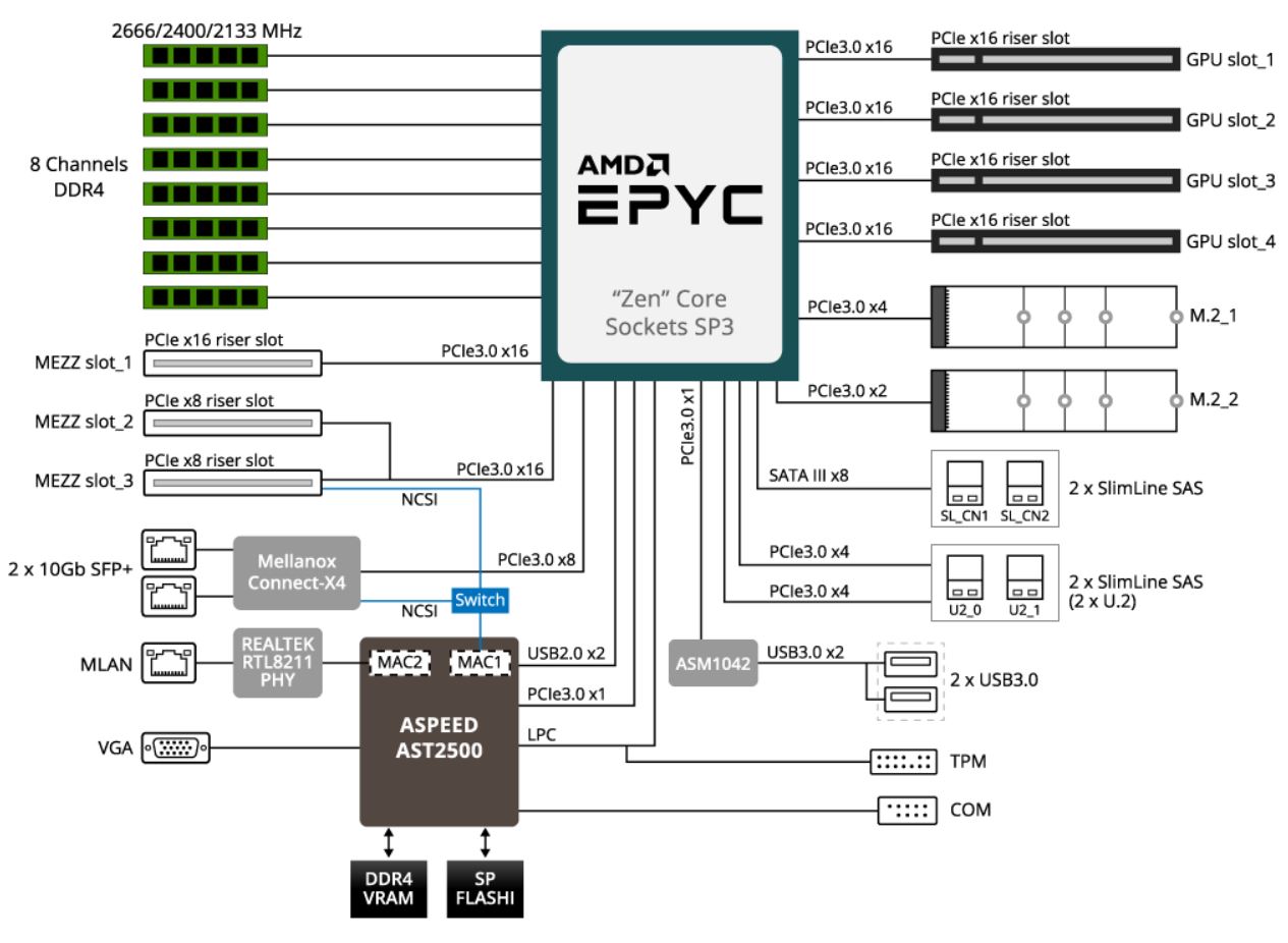
A common reason is that current platforms still include SATA, which the EPYC 7001 can support via its I/O lanes. Another key reason is the BMC. Adding a BMC to an AMD EPYC 7001 lane can take away three other lanes from NVMe storage which generally uses x4 lanes. You can see that there is a PCIe 3.0 x2 M.2 slot, to help uses the remaining lanes since the ASPEED AST2500 is using an x1 lane. This block diagram shows the impact of adding the BMC as we conceptually showed in our diagram above.
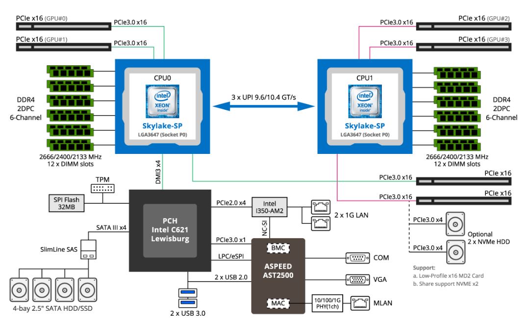
Server BMCs are ubiquitous, and they use PCIe to connect to the system. By moving that PCIe x1 connection off the main lane sets, it creates a cleaner solution for motherboard re-spins. If you recall from earlier in this article, Intel has the Lewisburg PCH with its own SATA and PCIe lanes that often handle the BMC connectivity. Here is an example using an Intel-based Gigabyte G191-H44.
For newer platform spins, that can mean 129 PCIe lanes for a single socket CPU or 130 / 162 lanes for dual socket AMD EPYC Rome systems. We do not expect this to be available to current AMD EPYC platforms since the lanes and platforms are already set.
Assuming we do see uptake on this feature, it will open up the AMD EPYC Rome generation to have even better PCIe connectivity. With Dell EMC PowerEdge BOSS-like cards for SATA boot drive connectivity as well as NVMe proliferation, this could be a great way to modernize the AMD EPYC platform.
Update 05-April-2019: Everyone seems to be calling this feature WAFL.
Final Words
Putting this into perspective, AMD’s strategy is looking very strong. Seeing the Gen3 to Gen4 transition, one can imagine that a similar architecture in the future can scale to Gen5 (via another board re-spin) doubling performance yet again. This is a vastly different strategy to Intel UPI and the increase in bandwidth is scaling much faster for AMD. In this generation, Intel left UPI at 10.4GT/s which is the first time it has failed to increment QPI/ UPI speeds in the last decade.
For most systems, the less sexy 129/130 numbers are actually the most exciting. The addition of auxiliary I/O lane(s) means that one can add more higher-speed PCIe devices like NVMe SSDs or GPUs to a system.
This article has been in the works for a few weeks and I did give AMD the heads-up that it would be going live just after the Cascade Lake launch. They did not sanction this article (indeed, they will not be overly excited to see it is live.) I wanted to ensure that we could compare AMD’s plan to the actual number for the new Intel platforms that we were under embargo for at the time this is being written. Now that we can discuss Intel’s mainstream 2019 platform, we wanted to bring up the coming competition. Things may change between today and the actual launch. As always, there is an asterisk here until the platform ships from AMD and its partners.
For the record, knowing the above and armed with benchmark data we had already generated on 2nd Gen Intel Xeon Scalable, we purchased several AMD EPYC platforms for our infrastructure the week before the new Xeon launch. We will add Xeon Gold with Optane DCPMM in the coming quarter as well simply because DCPMM memory mode is very useful to us.
Intel has been shipping Cascade Lake for revenue for months while the AMD EPYC Rome generation is not publicly available. There is always something better coming and Intel made major gains against AMD EPYC 7001 with this generation. 2019 is shaping up to be an exciting year and Rome is leading the way toward a modern architecture.


So there’s fewer links dedicated to package-to-package communication that frees up some for PCIe.
That’s great, but AMD made a huge deal about the “socket compatibility” of these new Epycs… aside from the fact that PCIe 4.0 ain’t going to work on an old motherboard without the repeater chips, an old motherboard also won’t rewire itself do deliver all these lanes.
On top of that, how practical is it to be using all of these lanes in a real-world 1U or 2U server anyway?
This is really smart by AMD’s engineers.
Don C – they’ve addressed those points in the article p. 2
I wouldn’t believe it otherwise, but this guy is the #1 server bro in the world right now.
That sounds like a real winner so long as the rome cores don’t suck and the io die to core isn’t crippling
Regarding socket compatibility, are there extra pins on Epyc’s socket that were unused with Naples but would now be defined as PCIe contacts for Rome to enable this bonus PCIe lane?
We buy servers fully integrated in racks, so this is far down the stack from what I’m usually dealing with.
You’ve done a good job dumbing down the explanation so someone who doesn’t come from hardware engineering can understand what they’re doing.
Jonathan they’ve even got GPIO from the SCH that they can use.
As my kids say “yeet” AMD. Cascade’s been out hours and already looks like a dinosaur.
Only one thing left to wonder about, how fast is the connection between the chiplets and the I/O die? I think it’s a very clever design to get around the limitations posed by NUMA with first generation EPYC, it is somewhat ironic that Intel is moving in the opposite direction putting two separate dice into the high end Cascade Lake CPUs.
I can’t help but question the utility of this cpu package interconnect. Amd can create as much bandwidth as they like between cpu packages but all that bandwidth is totally wasted with CPUs that clock at around 2.2 – 2.6GHz while Intel is already selling 3.8-4.0+ Xeons that run on such speed for dozens of cores. Either workload is CPU bound or it is not. When it is then CPU tacts matter and the interconnect bandwidth is not that important anymore. All AMD is doing is removing the past bottleneck but they still hugely under perform Xeons. I see zero applicability for HPC workloads.
The only HPC benefit I can see is that you could now do 8 GPUs and 2 nics in a system at twice the bandwidth to the CPUs as Intel, and you don’t need pcie switches which the HPC codes don’t like.
If AMD’s got faster memory 3200 rumored and gen4 that’s a lot of good before knowing what the CPU pipeline
Honestly I never tire of touching myself because I’m such a fanboy.
@Matthias Wolf: You realize that AMD can also sell lower core-count parts clocked higher if that’s what you want, right? AMD has had no problems hitting 3.5GHz on Zen so there’s no reason to expect they’d backpedal on that now.
Re. HPC, IDK, I thought a big chunk of HPC cared about DRAM bandwidth; a bigger chunk than those that care about peak flops. 8-channels > 6-channels no? Yes, there’s cascade lake AP to post high scores on benchmarks, but that’s a completely new board. And HPC still connects I/O like Infiniband, Storage, no?
“but they still hugely under perform Xeons” In what? Linpack? Sure. Generally? Not “hugely” and this is speaking of Sky/Cascade vs Zen. Recall nobody without an NDA has seen Zen 2 yet.
@Don Cornelius: AMD’s stated objective with Zen/Naples was to replace low/mid core-count 2P intel systems with a 1P naples. Hence the I/O. Apparently many folks bought 2P because 1P XCC was too expensive and didn’t have enough memory/I/O (so say AMD marketing, so pinch of salt and all that, but it sounds plausible). View it in the light of that fact. If the only reason you were 2P was to get gobs of I/O, you now have a solution in 1P. If you really needed lots of memory channels and memory in addition to lots of cores, 1P is probably not for you. You could extend the argument to 4P->2P consolidation although that’s a bit weaker.
Also, compatibility generally means backward compatibility in this business. My understanding is that Rome plugged into an older board will default to PCIe-3 which satisfies that definition. It is not as if newer features cannot be introduced (AVX123, TSX, etc).
@Matthias Wolf: While Intel is already hitting these high boost clock rates, they do so at the expense of a massive amount of power. Remember that Intel bases their TDP off of base clock, so with all cores running at 2.5GHz the 8180M uses 205W, once it boosts their TDP can easily double so that 205W becomes 410W. Now with the new 56C it has a 400W TDP which means while boosting each socket could pull 800W! Your 2 socket server with any cards/drives in it will need a 2000W PSU minimum. AMD does have their 16C high core clock Epyc and it looks excellent. I would assume they will do the same thing with the Epyc 2 line but perhaps have higher core variants.
@Jeremy: The 8180 can sustain up to 3.2GHz on all 28 cores in some non-AVX workloads. But these are nowhere near 3.8-4.0GHz on dozens of cores that Matthias Wolf claims. Intel ups the 8280 all core turbo boost to 3.3GHz and the 4GHz turbo is only achieved on 2 cores.
“the release of the “Cascade Lake” series of Intel Xeon Scalable processors”
Amazing, Intel can keep selling products and even market new products that all have the “Spoiler” security hole with NO effective patch, and people keep enjoying paying more for “Spoiler Inside”!
Researchers discover and abuse new undocumented feature in Intel chipsets
Researchers find new Intel VISA (Visualization of Internal Signals Architecture) debugging technology.
ZDnet March 29, 2019
Hard times for intel and it’s followers.
AMD document 54945 “PPR for AMD Family 17h Model 01h B1” lists WAFL PCS w/ x2 E12G PHY in chapter 1.7 Processor Overview. Did Naples already have these “WAFL Bonus PCIe Lane(s)”?
@deltaFx2, AMD never did with previous server CPUs. Can? Perhaps but perhaps not. Tact frequencies on most all previous server CPUs by AMD underperformed Intel on an equal core count comparison basis. Memory speed and bandwidth is almost always of lesser priority than cpu tact frequencies in hpc space. And Intels avx512 blows amd away in that category as well. HPC hugely depends on high tact frequencies, I also know a lot of houses that work in deep learning space and run gpu compute servers and require among gpu cards fast CPUs because some of the workload is cpu bound. As I said Rome may lend itself well to certain areas but it’s not gonna be hpc or gpu compute
@Jeremy,@Alex, all right not dozens but 18 cores (6154) and 12 cores (6146), at a top 3.7ghz and 4.2 ghrz respectively. Multiply cores by 2 as those are being deployed on dual socket boards and you get your dozens. Amd only countered in November last year and even that epic chip performed poorly (7371) vs my other 6146 and 6154 Intel chips in most math computations. There is a reason that as of today hardly any hpc or gpu compute vendor utilizes epyc chips despite their high pcie lane count.
@Matthias Wolf
dare to explain this then? https://www.hlrs.de/whats-new/news/detail-view/2018-11-13/
As an HPC User I am quite intrigued by the new AMD CPUs for the following reasions:
1) Two full AVX-2 lanes
2) No downclocking, as on Intel CPUs, when AVX is fully activated.
This article has good info, but could have been written in 2 paragraphs.
Making an article unnecessarily long is wasting readers’ time. Less is more.
@Matthias Wolf:
“Memory speed and bandwidth is almost always of lesser priority than cpu tact frequencies in hpc space” Really?Take a look at this: https://arxiv.org/abs/1810.09330 “Double-precision FPUs in High-Performance Computing: an Embarrassment of Riches?” They conclude that 60-70% of HPC loads they run (RIKEN) are memory bound. I’ve also read someone from Berkeley complain about modern CPUs being optimized for cloud/enterprise vs. HPC on the memory side but I can’t find a citation now. It may well be that what you do fits well in the caches (DGEMM etc) but it’s a huge generalization from one datapoint. Also, HPC != Deep learning. There’s some overlap but in my view, HPC is Double Precision stuff. Moreover, you’re complaining about an unreleased product stack.
Unless you can get >50% utilization of FP 512 units, you are not going to be much better than AVX-256 (full width) for a given application. There are loads that can do this (*GEMM, Linpack, etc) but it’s hardly the norm. This is also why AMD is able to keep up with Xeon in SpecFP; spec FP is mostly memory bound. FP 512 is great to post linpack scores on Top500. And there certainly will be loads that vectorize well and fit in the caches. To me, AVX-512 seems an attempt to keep nVidia out of the datacenter.
As to who in HPC has signed up for rome, take a look at this: https://www.hpcwire.com/2018/10/30/cray-unveils-shasta-lands-nersc-9-contract/ And they’re not the only one.
L. P., I never claimed that nobody finds utility in this chip for HPC. I made a generalized statement. Your link provides no details how those nodes that will run on Rome CPUs is utilized. I can assure you that that not a single machine that makes use of cpu bound traffic in high frequency trading, a show case of hpc, where latencies and high throughout really matter, utilizes Epyc chips. I know of not a single one and consider myself relatively informed in this space. Are there use cases for epyc chips? For sure. But as I said, it depends specifically which workloads. Even a super computer cluster has various workloads and for some of it fpga cards make the most sense, for others high performant CPUs and for again others you want Chips with lots of pcie lanes. The article you quoted does not go into any detail on the precise use case where the Rome chips are supposed to be utilized.
@deltaFx2, I am not judging from just one data point. I am pretty well connected in the high frequency trading space where there are either fpga or cpu bound workloads involved and where nobody cares about AMD (so far) because they have no product that remotely competes with Intel or fits minimum requirements. There are now a few epyc based gpu servers out there but the large majority runs on E5 v4 machines or Xeon scalable chips. Does that constitute the entire hpc space? Certainly not, but it represents typical use cases in hpc space.
Furthermore, I have the Xeon Gold 6154 and Gold 6146 and both outperform the Epyc 7371 in various applications that involve cpu compute without any specialized optimizations on the software side for the Intel CPUs. I can’t speak for Rome as they are not out yet but I am prepared to be disappointed. Again, I am working in a nich area and can’t speak for the utility of those chips in network, web, or storage related applications. I welcome competition and hope amd eventually gets its act together. But I find the amd hype by fan boys completely over the top. Many even claim how Amd is gonna heavily eat into Nvidia’s market share in gpu space. Those are dreams and wishes but none of that is validated by trends or statistics. Equally in gpu space, AMD does not have competing products that come close in performance to what Nvidia offers in the top segment. Not even remotely close.
@Matthias
EPYC Rome has 4x the AVX performance compared to EPYC Naples, EPYC Rome has twice the L3-cache compared to EPYC Naples. Xeon Gold 6154 cost $3500, Xeon Gold cost 6146 cost $3300 where EPYC 7371 only cost $1700.
@Micha, it’s interesting that you are one of the first who mentions price because surely this category is a clear AMD win. No disagreement here. Am quite curious about the Rome AVX performance because many of my cpu bound apps peruse avx. The only way to find out is to try out. Marketing gibberish got me into the early threadripper gen1 then gen2 then epyc gen1 and all disappointed big time. I only speak for the applications that I used to benchmark performance,among many others, C++ compiled code (I used ICC but also other non Intel ones).
Would it be possible for AMD to tap those extra PCIe lanes into more sockets? 4p or 8p?
@Matthias: “Does that constitute the entire hpc space? Certainly not, but it represents typical use cases in hpc space.” Now here’s where we fundamentally disagree. You’re probably the first person I’ve come across who classifies high frequency trading as HPC. It’s an interesting argument, but HPC to me means large clusters often running MPI, solving large-scale science problems (CFD, particle physics, molecular biology, that sort of thing). And I do think trading workloads does not represent HPC workloads; trading workloads are strongly incentivised to shave off the last microsecond, something HPC does not have as strong an incentive for. My original point stands: you said “I see zero applicability for HPC workloads.” You meant “I see zero applicability for high frequency trading”. You may well be right, but you are extrapolating from one highly biased sample (I’ll grant it’s not one datapoint but several similar ones). It may also be that your application is highly tuned over the years for intel’s cache hierarchy (and it’s totally reasonable to go with intel at that point).
I don’t know or care about market shares in gpu/cpu. I just found your original claim of zero applicability very strong.
@deltaFx2, https://www.hpcwire.com/solution_content/hpe/financial-services/big-data-hpc-speeding-innovation-high-frequency-trading/
Hft is definitely part of HPC, regardless of how you or I feel about it. So are GPU compute servers. When you just look at above two areas they make up orders of magnitudes more machines than the hpc use case you described. So I guess you took issue with my points because you were slightly confused about the definition of HPC and what it encompasses. Having said that, perhaps look at hft machines or check out Supermicro and their gpu compute server products, how many Epyc based boards do you see? Same with most other vendors. I start to get the impression you just like to disagree. Epyc 7371 benchmarks vs Intel CPUs are in public domain, check them out (specifically vector compute) . I myself benchmarked the CPUs with all the applications that I need to run efficiently. Then you have hardware vendors in hpc space that stayed mostly away from Epyc chips. I am talking about facts here not your or my feelings. Let’s agree to disagree at this point and if I hurt your feelings with “zero applicability” then I apologize and happily correct it to “currently low applicability”
@Matthias You do realize that your purported conclusion is actually contradicted by your cited reference?
The logic behind the article is big data and hpc influencing high frequency trading. Not the other way around. The article furthermore treats all three areas as separate entities hence leading your conclusion ad absurdum.
@L.P., AMD itself promotes the Epyc 7371 as Chip useful for high frequency trading applications :-) AMD itself said it. And AMD sales was quoted in interviews with Anand tech. Anyone working in this space acknowledges that gpu compute and hft are both part of hpc. I pointed to the sources, feel free to look it up. And if you still disagree then, we’ll, let’s agree to disagree. I own several Xeon gold and the epyc 7371 and have run performance benchmarks. Have you? I also work in hft space and spend many hours each day on deep learning networks. I acknowledged the areas I have zero expertise in, but claim to know a thing or two about what I have been doing over the past 11 years. If Rome will solve your problem then by all means go for it. I am absolutely convinced it will not be widely accepted in hpc space.
I think you are missing the point… are you sure the topologies are going to be like that??
I have yet to read an article to explain some fundamental e crucial things about Rome and the all 3000 lineup (since all Will have chiplets + central hub, AM4 sockets is already comfirmed, debuts with 1 chiplet but has space and provisions for 2 chiplets for the high-end SKUs -> meaning all DDR channel are also attached to the I/O hub) .
. The chiplets are tiny compare with the central I/OHub which is absolutly huge (it ocupies more área than the 8 chiplets, attending the individual packaging penaltis in area, no matter if the big is 14nm or half density)
. The 8 DDR RAM channels are all directly attached to the central hub e none to any of the chiplets, i. e., the tradicional cpu-memory paradigma is decoupled… for the first time in modern times,..
https://wccftech.com/amd-epyc-rome-zen-2-7nm-server-cpu-162-pcie-gen-4-lanes-report/ for purposes of ilustration i picked the first link, but the graffic is AMD.
. In such a topology you don’t need a x16 lane link to connect to other chip/chiplets that also had direct attachement to DDR RAM, as in the previous solutions and topologies of AMD… now the all memory traffic comes from a central location… and the same lane provision in HT or Infinity Fabric, of previous iterations, is sufficient for each Chiplet (previous chips or dies in a socket) to connect to all other 15 chiplets in 2 sockets, if each x16 links can be divided in x4 (they all now only snoop caches in the background and respective very low traffic)… 3 x16 links outside Socket, is 1 x16 for the other central I/O hub, and 8 x4 for the other chiplets-> meaning all chiplets comunicantes with each other even with 2 sockets.
The 1th time i saw it… ‘wtf, huge mistake’… AMD many times is ahead of time, but others also do huge poo… 8 chiplets with 64 cores, all ‘fighting’ for memory resouces at a central hub, simply the “contention” must BE huge (more so in 2 sockets, because requests for memory can came also from the other socket) … unless there are many ways to mitigate this, which invariably passes for having the chiplets caches very well “warm up”, among some other things… Neither of this can PCIe provide or does it matter how many links, or if is gen 4 or 4K…
From what i researched PCIe absolutly can’t cope with it, but Gen-Z can…
https://genzconsortium.org/educational-materials/
Gen-Z have an “abstract physical layer”, treats at first everything as Just a Bunch of Lanes, and the “magic” is in the “Gen-Z Core” wich then knows what to do with those Lanes that attach it. Each Gen-Z core, were a Bunch of Lanes attach (no matter topology, sinal rates or modulation, i.e., NZR or PAM4), can BE parte of a “component media”, wich can be a single “device” or a collection of devices with many functions (compute, special acceleration, memory, etc), and it already support with its ‘memory semantic and plural messaging’ much more than 2000 functions, including all of the PCI/PCIe up to Gen5, that are a little more than 200 (CXL will be quite easy to have, the same with HyperTransport kind of “Cache Coerency”, which is the base for Infinity Fabric (also), and more, cause it as provisions, althought it doesn’t enforce any cache coerency, neither memory coerency for that matter, cause this depende on the implementers having the MMU/ZMMU with Address Translation, and Page Walking upon lists or matrixes, on the side of their “component device(s)”, and Cache Coherency mechanisms, on each side of a link, and goes further than the tradicional MOESI or actual MOWESI of AMD, everything is there, but depends on how or how much do you want, cause system are not going to be so simple anymore)… and all functions of PCI/PCIe cause ech G-Core takes over as a “Root Complex”, with each Device implemented in a “logic” way of extension (better than bridges), called LPD (Logic PCI Device), meaning they are already virtualized (even if it is mostly hardware), including the safe way of PCIe (Each G Core can have up to 2000 LPDs, huge collection of VMs or Containers on a server)… and a “collection” of DDR channels, connected to a Gen-Z Core, can be a “component media” also and have 100ths of adicional functions -> in the way of a data centric FULLY COMPOSABLE sistems… and connect to 1 or more switches that serve many other “components”…
Bottom line: you can have a sistem with only PCIe defined slots, attachements, etc, including U3 (with a HBA or not) and U2 for storage… but the underlayind traffic that goes behind the sceanes, is almost all Gen-Z… even having a REGULAR/NORMAL x16 adapter, Gen III or IV doesn’t matter, enjoying already up to 32 Gbps/lane, and all the 100ths of additional functions, including Memory Coerency and Cache Coherency, and as many as the adapter can support and the system offers (that is, a regular PCI-E adapter, can already be accelerated, by sitting on a PCIe slot on a system that has Gen-Z behind the all routing and interconnet, restrion being if it enforces PCI ordering PCO) (Imagine a GPU adapter, that is regular PCIe, but is also able to work with Gen-Z and all its possibilities -> https://community.amd.com/community/radeon-instinct-accelerators/blog/2018/11/13/introducing-the-world-s-first-7nm-gpu-and-fastest-double-precision-pcie-card -> 4 GPGPU cards tied togheter by Infinity Fabric, having cache and memory (their internal) coherency as one… then sitting as nothing more than regular PCIe slots, is a wast that does compute… I don’t think AMD as gone this far, all around Gen-Z no matter if all attachments are “legacy” … yet… but in here i hope there is the real bonus ).
For alleviatting Memory Media contention, there is buffer/cache with “pattern recognition”, wich can be stride for pre-fetch, regular expressions etc… and there is a possibility of called “Collective Processores”, at each switch on the Fabric, and that treats the Requests/Responses of the Collective component medias attached to that switch as a single entity (for sure alleviates contention and imposes more order on a link) …
Comments are closed.