
The Intel Xeon Max processor is part of the company’s new branding for HPC products. Along with the Max GPU series, the new Xeon Max CPUs are optimized for HPC deployments. In this generation, this is the product previously known as “Sapphire Rapids HBM” combining a next-gen Xeon CPU with HBM onboard to increase memory bandwidth for HPC applications.
Intel Xeon Max CPU is the Sapphire Rapids HBM Line
Intel notes that many HPC applications are memory bandwidth limited. Extracting the most performance from a processor is often limited by getting data to cores, rather than the performance of each core. As a result, there is an opportunity for faster performance using faster memory. We will quickly note here that AMD is going to increase the bandwdith per core in its upcoming “Genoa” chip that we will discuss tomorrow.
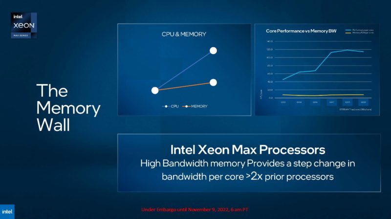
According to the new disclosure, the Intel Xeon Max series of processors will only scale to 56 cores, not the 60 core non-HBM units that we tested recently. That acceleration will be a key part of the new generation. There will be 64GB of HBM2e onboard and Intel will be over 100MB of L3 cache with up to 112.5MB. Another notable feature is that the new chips will scale up to 2 sockets even though the Sapphire Rapids line will scale to 4 and 8-socket systems. 1-2-sockets is the mainstream HPC design these days.
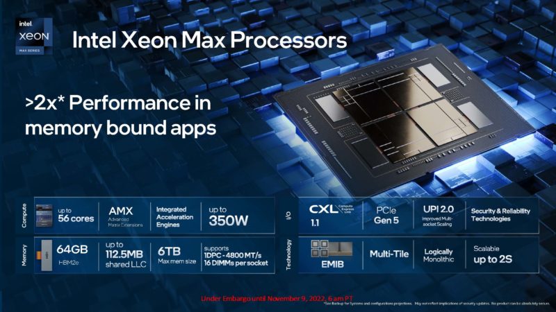
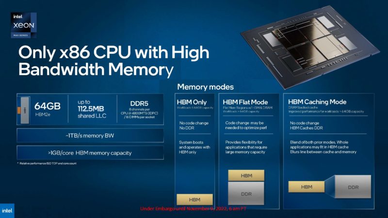
Intel expects over 1TB/s of memory bandwdith from the solution. There are three modes the chips can run in. One will be that there can be HBM Only, where no DIMM slots are populated. That limits memory capacity to 64GB per CPU but saves the power and cost of DDR5 as an offset. The HBM Flat mode treats HBM seperate from DDR memory giving a fast and a slower tier of memory. Finally, there is HBM Caching mode where data is cached in the HBM memory and that is transparent to the host. Intel has had a similar memory scheme with Intel Xeon Phi x200 in the past, albeit now the fast memory is HBM. Intel also used tiered DRAM caching with Intel Optane DIMMs. See the video on how Optane works here as well.
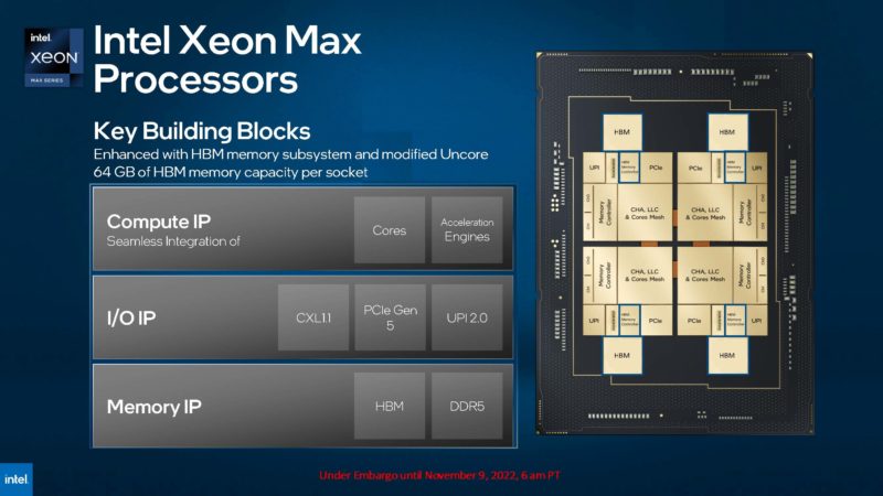
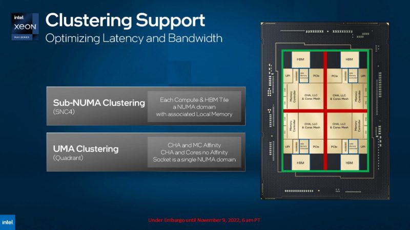
Intel is showing the Xeon Max processors as a collection of IP. In the Ponte Vecchio GPUs, now named the Data Center GPU Max series, there are many tiles making up different types of IP. In the Xeon Max, Intel has the x86 cores, local caches, PCIe Gen5/ CXL, UPI, accelerators and memory controllers on four tiles. Each has a connectin to a HBM stack. The tiles are then connected to neighbors to build the larger CPUs.
Intel has its newer P-cores in the design.
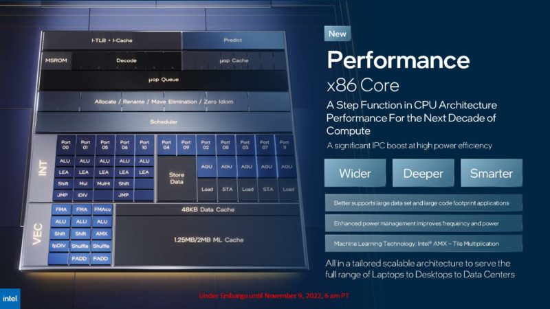
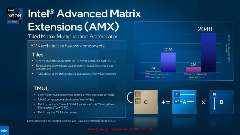
Intel also has AMX. Intel AMX helps in matrix multiplication. We have already shown some of the impact of AMX in Hands-on Benchmarking with Intel Sapphire Rapids Xeon Accelerators, albeit that was with dual 60-core CPUs.
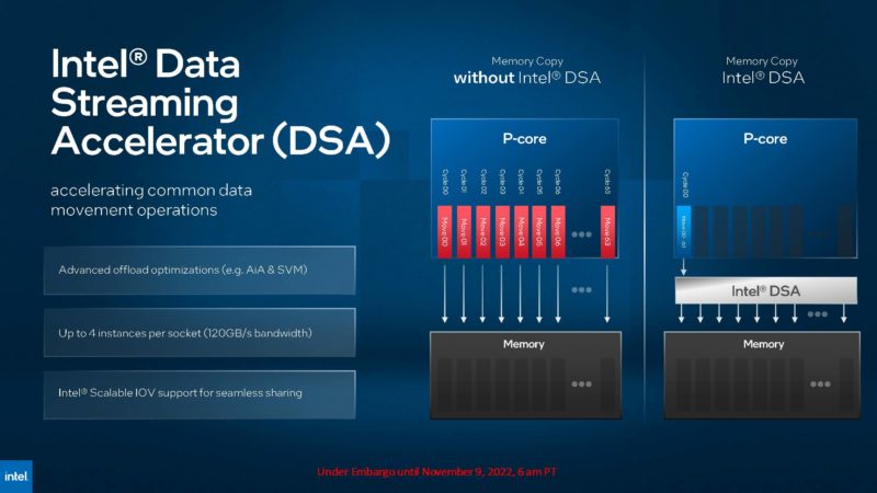
The Intel DSA helps offload data movement tasks. Intel has been talking to us a lot about DSA, so this seems like it may be a big feature.
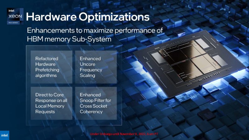
Aside from that, Intel has a number of hardware optimizations that you can read in the slide below.
Intel will have both sub-NUMA clustering and UMA clustering in this design. This is important as it allows cores to work directly with HBM and local DDR5 on the same compute tile as the x86 cores. Using these modes allows applications to minimize the data movement across the chip and therefore increase performance.
The 5x performance gain is a strange one here as that is using Stream Triad, a memory speed benchmark, that would be most sensitive to memory bandwidth since that is what it is measuring. Intel is using the AMD EPYC 7773X as its comparison point. That has 768MB of L3 cache based on “Milan”. This is the correct comparison point since AMD EPYC Genoa launches tomorrow. Genoa will add AVX-512 and a 50% increase in cores. Genoa-X we expect will have >1GB of L3 cache and will likely launch in the first half of 2023, within a few months of Xeon Max. We expect that chip to be much faster than the EPYC 7773X.
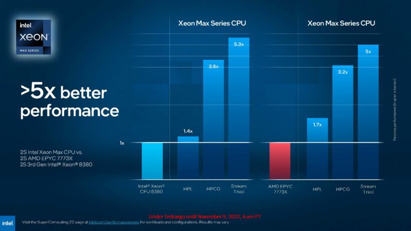
Again, Intel is comparing its performance to the Milan-X EPYC 7773X. That is the correct comparison today. We will show some performance and discuss more tomorrow, but the new EPYC chips are a massive jump from the older ones.
Timing is fun on these things.
Final Words
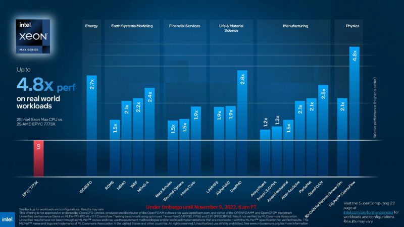
We expect the next generation of HPC-focused CPUs to be really interesting. AMD will have a large lead on core counts versus Xeon Max. AMD Genoa-X we expect to be well over 1GB/ L3 cache per core while also offering up to 50% more DDR5 bandwidth. Xeon Max is using fast and relatively large on-package memory instead of growing caches. We will likely see some workloads that have random data sets too large for AMD’s caches look relatively spectacular on Xeon Max.
Intel told us that Xeon Max will use the full 4 compute tile design across all of its SKUs. We think this is required for four packages of HBM 2e. That means it will not use some of the lower-core counts Sapphire Rapids designs that are notably different from the larger chips. Also, given Intel is saying that Xeon Max scales to only 56 cores in 350W, it seems like one is trading maximum core counts for HBM. HBM also uses significant amounts of power, so we were a bit surprised by the 350W target given where AMD will be with Genoa.
Perhaps the exciting thing is that we are now seeing not just favored HPC SKUs out of a broader SKU stack. Instead, we are seeing designs looking to address the challenges of keeping cores fed with data.


Question to Intel marketing: so what comes next, after max? ;)
Is this going to be only for XCC dies, or MCC as well?
Looks like onboard HBM is positioned as the performant brother on the other side of the DIMM for tiered memory.
I suppose they could pull an Apple can use “Ultra”.
Also, if there isn’t much margin for growth in the current package, I suppose it would be at max headroom.
“AMD Genoa-X we expect to be well over 1GB/ L3 cache per core”
Really? So a 128-core CPU will have 128GB of L3? That seems very improbable.
The decision to refrain from activating all 60 cores on dies makes me seriously worried about the state of Intels 10nm. Ice was rumored to be 38 forever, and they increased it there too, probably because of pressure from marketing. There will be some rather painful HPC benchmarks where memory bandwidth is not the be all and end all, and the 60 core SKU will win.
Are these socket-compatible with other sapphire rapids Xeons, or are those little ‘ears’ either mechanically incompatible with the usual socket or used for extra lands that need a correspondingly larger socket?
@ssnseawolf
Judging from history, it’s probably only on XCC dies due to a lack of space for I/O balls on smaller dies. OmniPath was only on XCC dies for example.
@fuzzyfuzzyfungus
Look at how OmniPath (F) enabled LGA3647 CPUs had the connector stick out of the socket.
I presume this will be the same with the LGA4677 socket since the socket doesn’t have high “walls” on the top and bottom.
After “Max” it’ll be “Amazeballs”
@Jure
Beyond Socketdome, Masterblaster,
Intel Xeon Max will give you wings
Meant to also add….Auntie’s Choice
Comments are closed.