
Perhaps one of the most hotly anticipated releases for the server space in December 2017 is the Intel Nervana Neural Network Processor. The Intel Nervana NNP is essentially the company’s answer to the NVIDIA GPU. This week, Intel showed off a NNP as well as provided more details on the chip.
Intel Nervana NNP
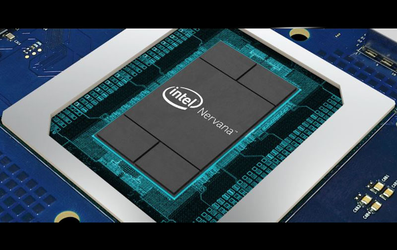
So what is the Intel Nervana NNP. In short, it is a custom hardware solution targeted solely at neural network training. It is custom compute silicon along with HBM memory at its heart. The basic idea is that instead of taking an x86 core where you have a legacy operational model, or a GPU where you start from a graphics processor (albeit now with a Tensor core accelerator), you have an architecture designed for the math of training. This is a deep learning ASIC with Intel investing in the ecosystem behind the ASIC.
Intel recently disclosed more on the NNP. Here is an excerpt from the release:
Spatial architecture
The NNP gives software the flexibility to directly manage data locality, both within the processing elements and in the high bandwidth memory (HBM) itself. Tensors can be split across HBM modules in order to ensure that in-memory data is always closest to the relevant compute elements. This minimizes data movement across the die, saving power and reducing on-die congestion. Similarly, software can determine which blocks of data are stored long-term inside the processing elements, saving more power by reducing data movement to and from external memory.
HBM is at the forefront of memory technology, supporting up to 1TB/s of bandwidth between the compute elements and the large (16-32GB) external memory. But even with this large amount of memory bandwidth, deep learning workloads can easily become memory-limited. Until new memory technologies become available, it is important for deep learning compute architectures to use creative strategies that minimize data movement and maximize data re-use in order to leverage all of their computational resources. The NNP employs a number of these creative strategies, all under the control of software. The local memory of each processing element is large (>2MB each, with more than 30MB of local memory per chip). This larger on-die memory size reduces the number of times data needs to be read from memory, and enables local transforms that don’t affect the HBM subsystem. After data is loaded into the local memory of each processing element, it can then be moved to other processing elements without re-visiting the HBM, leaving more HBM bandwidth available for pre-fetching the tensor for the next operation. Tensors can even be sent off-die to neighboring chips directly from processing element to processing element, again without requiring a second trip in and out of the HBM subsystem. Even simple aspects of the architecture like free (zero-cycle) transpose are targeted at reducing the overall memory bandwidth.
Flexpoint numerics optimized for neural networks
We designed Flexpoint, the core numerical technology powering the NNP, in order to achieve results similar to FP32 while only using 16 bits of storage space. As opposed to FP16, we use all 16 bits for the mantissa, passing the exponent in the instruction. This new numeric format effectively doubles the memory bandwidth available on a system compared to FP32, and utilizes 16 bit integer multiply-accumulate logic which is more power efficient than even FP16.
Flexpoint is modular. While our first generation NNP focuses on 16b multipliers with a 5b exponent, future silicon will enable even smaller bit widths in order to save even more power.
New forms of parallelism
The NNP includes high speed serdes which enable more than a terabit-per-second of bidirectional off-chip bandwidth. Similar to our memory subsystem, this bandwidth is fully software- controlled. QOS can be maintained on each individual link using software-configurable, adjustable-bandwidth virtual channels and multiple priorities within each channel. Data can be moved between chips either between their HBM memories or directly from the processing elements. The high bandwidth enables model parallelism (a set of chips will combine together and act as if they are a single compute element), rather than data parallelism (where a job is split up along input data boundaries). The ability to move data directly from local to remote processing elements ensures that HBM reads can be reused as many times as possible, maximizing data re-use in memory-bound applications.
(Source: Intel)
If you are getting the sense that this is an ASIC that is designed primarily to scale up to a large number of ASICs in a cluster instead of 8x or 10x GPUs like we saw in some systems STH tested, you have the right idea.
What about Knights Mill?
At STH, we covered Knights Mill previously and showed hands-on time with the current generation Knights Landing. Knights Mill is an architecture, based on Xeon Phi, that will be released in December 2017. Knights Mill is traditional x86 tuned for deep learning workloads. Essentially, if you have a large scale-out HPC cluster with Knights Landing for traditional HPC, you can also use Knights Mill and Omni-Path to do scale-out training.


Custom solution? Maybe AMD Navi
No, this is custom silicon and architecture from the Nervana acquisition.
Its great,and its my pleasure to thank you for your explanations,when you were in Rwanda.
Wish you could come back,and educate us more.
Comments are closed.