
This is a second piece based on the Hot Chips 34 talk by Intel on Meteor Lake and its client strategy. We already covered Meteor Lake, so this is going to be a larger article about the disaggregated future. Make no mistake, this is a new era of chip design.
Intel Enters a New Era of Chiplets and Disaggregation with Meteor Lake
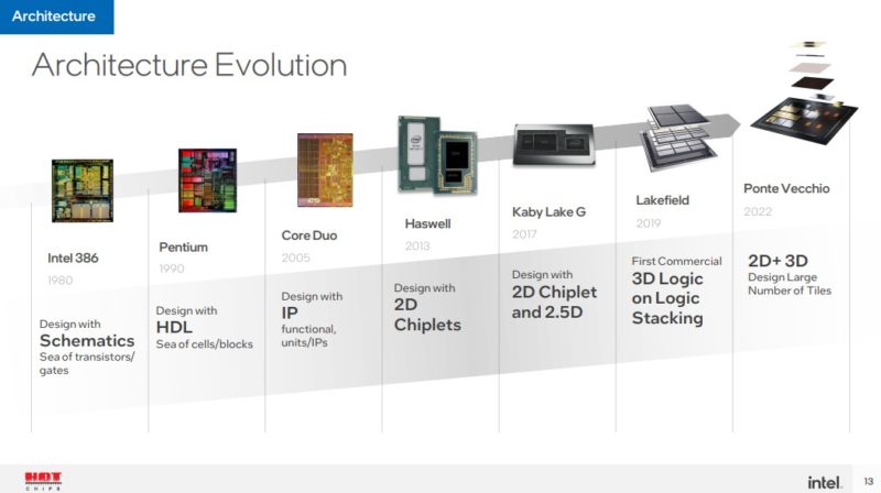
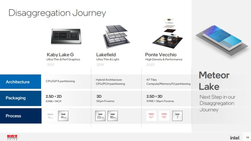
At Hot Chips 34 (2022) Intel discussed its journey from monolithic die chips that it produces for most of its segments today, to the disaggregated future.
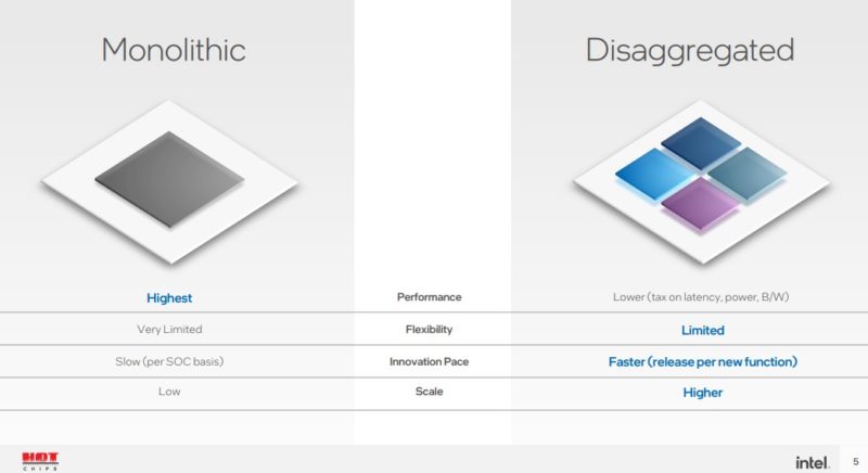
Intel has been co-packaging chips for some time. Intel Ponte Vecchio is perhaps the best example of where the company is heading with 47 different tiles integrated on a single package. Currently, that might be supported by high-end GPUs, but it may also be too much complexity in the client space where ASPs are much lower.
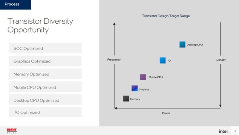
One item that Intel has been consistent on messaging since it started going down the tiled approach publicly is that different transistors optimally work on different processes. Moving to tiles allows Intel to match the transistor type to process.
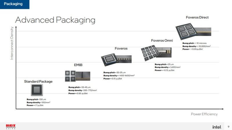
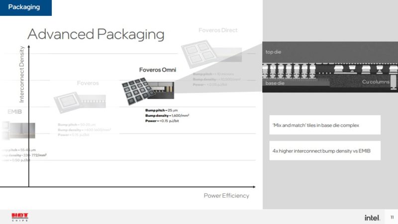
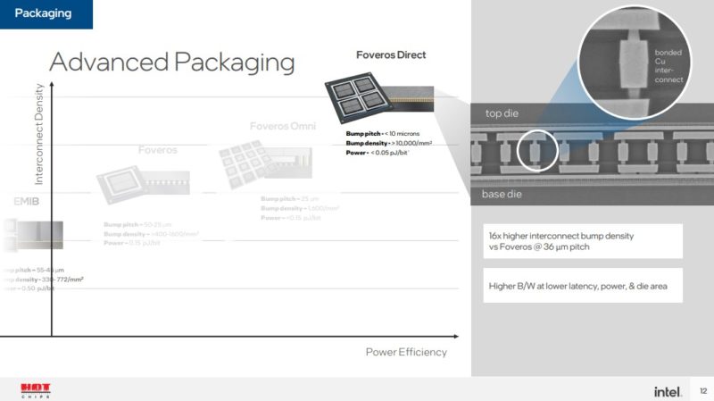
Intel also has a packaging line that spans 2D technologies as well as 3D technologies like its Foveros line.
Part of the challenge with doing consumer devices in tiles is that Intel needs to manufacture at scale. That means that Intel needs to have a process that is relatively low-cost to implement. Foveros is the line of technologies that Intel is using across much of its next-generation portfolio.
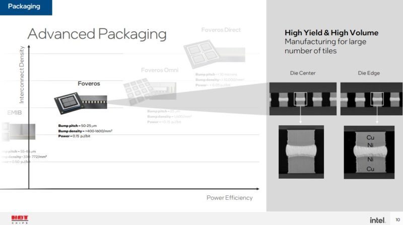
There are a number of Foveros generations and it has evolved since it was discussed at the 2018 Architecture Day.
The next generation gives more density to the connections but also lowers the power consumption of passing bits. This is critical as power per bit transferred (usually expressed as pJ/bit) can be a huge cost in multi-chip solutions. Power saved transferring data is power that can be re-purposed to doing work. In modern systems we often here anecdotes about the power of moving data through the system is greater than the power used doing useful work.
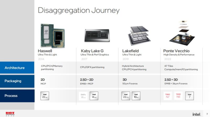
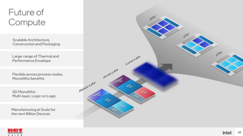
While Ponte Vecchio is the current high-water mark for processors we have seen, Intel is moving to a similar, yet scaled-down approach for its client chips.
Although we already covered Meteor Lake, we are going to use the slides as examples of what is going on.
Intel has a base tile that carries power and data connections up to the tiles that do work above.
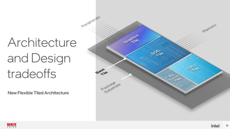
By changing to a tiled approach with this base die, there are trade-offs. The first one folks mention is cost. Intel says that the cost of adding the base die is relatively offset by the cost savings of being able to use smaller dies aligned to the most efficient processes. In the client space where CPUs compete on pricing that can have $10-20 deltas, adding $100 more to manufacture a chip in this manner is not feasible.
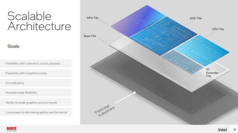
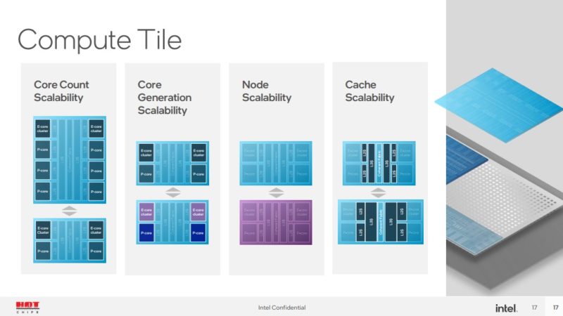
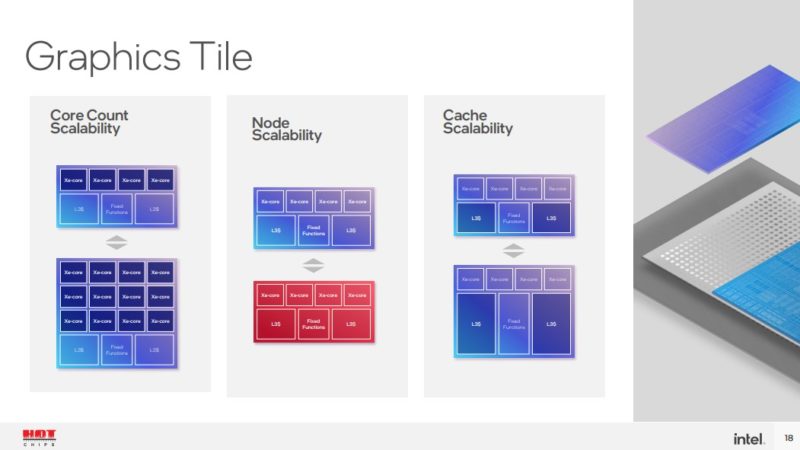
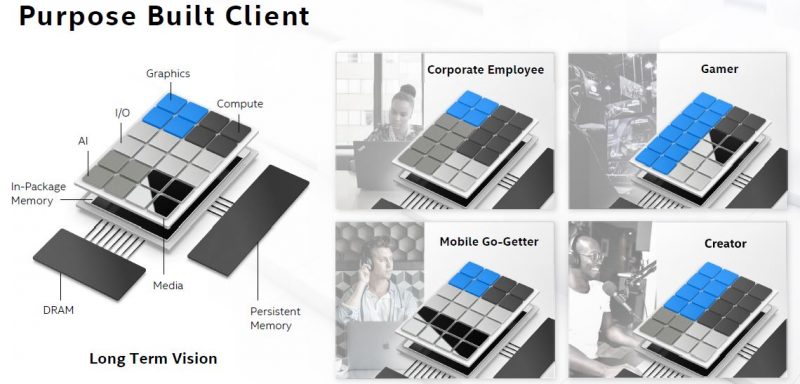
With this approach, Intel can design different compute tiles. Some may have different core counts and core types. Those tiles can also have different caches. Caches take up a significant amount of area on a tile. Having a compute tile with a relatively standard interface to the rest of the device means that Intel can innovate on new generations of cores or new generations of process nodes and then easily integrate them into existing products.
The graphics tile can similarly be revised over time.
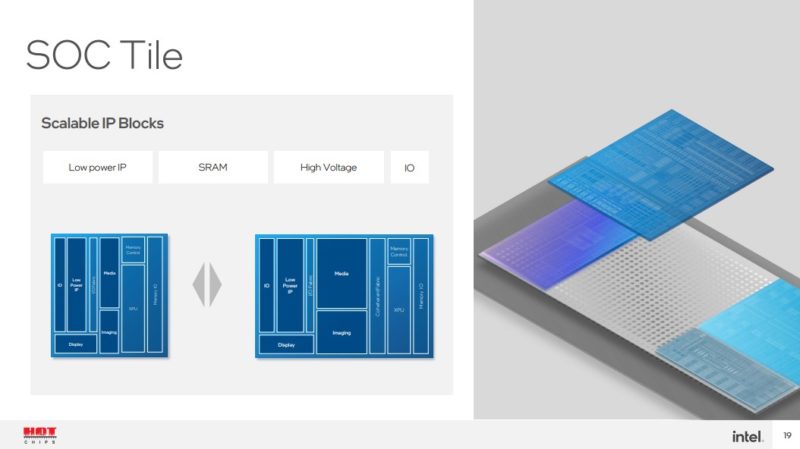
The SoC tile is interesting because Intel says the display, imaging, and media are better suited to this tile than the GPU tile. What Intel did not say, is that once there is a hardware accelerator, or there is display for perhaps four outputs, then this does not need to necessarily be changed with every generation. Pulling features out to the SoC that will span multiple generations means that Intel can focus efforts on revising the CPU and GPU tiles without having to validate that the display function works on a new process node that the future GPU is using as an example.
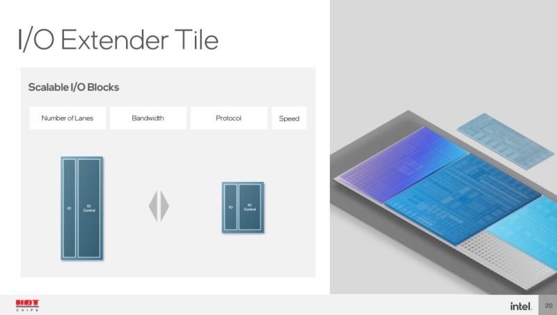
The I/O extender tile can be a number of things. Looking beyond Meteor Lake, features like PCIe Lanes, USB lanes, and more can be broken out into tiles and then integrated.
That is exactly where Intel was going with its cost discussion. As mentioned earlier, there is a “tax” in terms of disaggregating, but Intel believes it is relatively small.
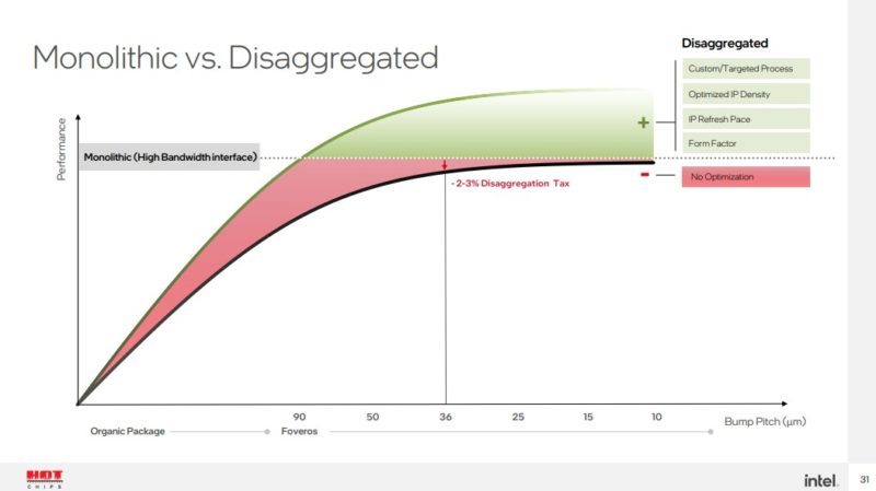
Intel also believes that by being able to target different types of process nodes for different types of tiles, it will help offset the disaggregation tax.
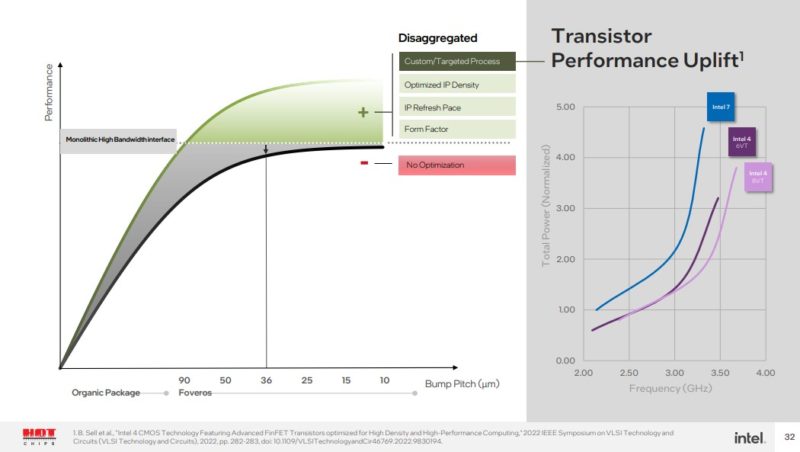
Intel also believes that being able to take advantage of new transistors sooner, it can help to offset the disaggregation tax as well.
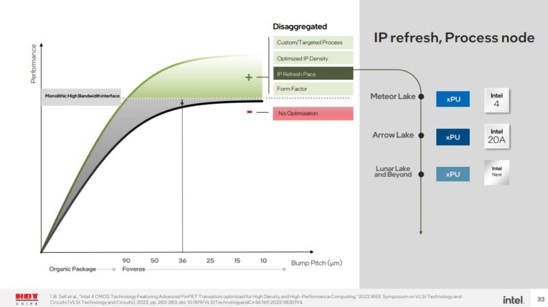
We will quickly note here that this is at a 36-micron bump pitch. At a 25-micron Foveros Direct level, that disaggregation impact would be even less. Given that, Intel did not get into Lunar Lake details, but its diagram shows an Arrow lake CPU/GPU tile refresh while keeping the SoC and I/O tiles. Lunar Lake is something different, but perhaps Intel already showed us the future.
Two years ago, we covered SoC Containerization A Future Intel Methodology. Much like how monolithic applications have been migrating to microservices, Intel is moving from monolithic dies to smaller tiles. Meteor Lake/ Arrow Lake looks a lot like an evolution of the 2020 era “Multiple Dies” from the IP/SOC Methodology Change”. The CPU is its own tile, the GPU is its own tile, but the I/O tile has been split into two.
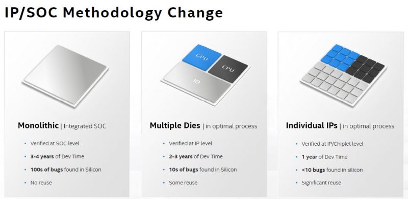
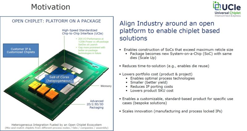
The next evolution Intel discussed was breaking things out to individual IPs. It could then make smaller chiplets. By doing so, it can then innovate faster on each IP. Intel’s product groups would then need to take the IP blocks and compose chips based on those IP blocks for different market segments.
Perhaps the more interesting aspect to this is not just what Intel is showing above, but then taking a step further and looking at its integration efforts. The company released UCIe which the industry is rapidly gravitating to in order to facilitate a chiplet ecosystem.
The implications of this are huge. For the consumer space, do we see more integration to the CPU package as it becomes less expensive to add I/O via I/O tiles (e.g. higher-speed networking, AI acceleration, or more?) Across Intel’s portfolio, will that mean that a Dell Core i9 has a different silicon tile integrated into it versus a HP or Lenovo tile?
Going beyond just the vendors themselves, this has a huge implication on how Intel will need to operate moving forward. Moving to a tiled approach may mean Intel can actually make highly differentiated solutions. A product manager instead of having to take the consumer Core-based die and then spec’ing ECC will be on and coming up with the speed and core count portfolio for the Xeon E series may be able to choose P-tiles, E-tiles, AI-tiles, networking tiles, I/O tiles, and all of them may not be from Intel. That is an enormously different task than the product teams have realistically done in the past.
For the market, that will bring a new dynamic. A VPN appliance vendor may be able to get a custom encryption chiplet integrated just for its machines. A HPE and Dell EMC server may use different flavors of Xeons. Perhaps a Dell Core i7 will no longer work in an ASUS Core i7 (this already happens with AMD PSB.) Are there market-specific requirements for accelerators on the I/O die that make chips region specific like Blu-ray’s?
Final Words
While Intel’s Hot Chips 34 talk was focused on its client Meteor Lake solution, the more impactful implication may be what it means for Intel, other companies in the industry, and Intel’s customers. If a true chiplet marketplace develops, then the pace at which we get new innovations can increase. It may also create chaos for largely structured markets that we have had for the past decade or two.


i still feel that Intel is a little late in seeing this potential and bringing it to market. These are ideas that hit me immediately when Intel was first showing them off 4 years ago to the public. However what they show to the public is known behind their closed doors long before we see it. Intel needed to pivot their roadmap then to avoid their 10 nm pitfall.
However the past has been written and this is genuinely exciting stuff to see. While the potentials on the compute and scalability side are real, what has me enthusiastic about the future with this technology is silicon photonics. Why worry about network interface cards or DPU acceleration when you can throw a slab of switching logic and a photonics die to built a many-to-many, high bandwidth, low latency network.
One other aspect missing from this presentation is that of memory. Types like HBM already leverage these packaging technologies to be integrated directly next to a compute die. While expensive, there is certainly a role for HBM in the highend. I would imagine that the ‘sea of cores’ is more akin to a checkerboard with half being mixed compute (CPU, GPU, AI, FPGA etc.) and the other half being a type of on package memory in a tiled topology. The result is that each compute die will have direct access to four memory stacks locally while the rest of the package is seen as remote: full NUMA in a package. The consumer side will also follow the checkerboard strategy as it’ll take up less board space, consume less power and offer increased performance vs. even stacked on package LPDDR5.
Speaking of interesting chip packaging, my wife’s Mac Studio Ultra finally showed up (it was ordered in late May)…And I visited my old comrades this week at what was a very Xeon shop, and saw the last beast I got to test there, Milan, in some quantity…”Rome wasn’t built in a day”, but it beat out the competing Xeons of the day to get AMD’s foot in the door of said facility.
The entire Hot Chips conference seemed like a marketing op for Intel. I know they are some kind of unobtanium-tier sponsor, but the mods didn’t have to skip every hardball question in chat.
It’s a bit funny to read about how chiplets will ~CHANGE EVERYTHING~ on this site too. Intel’s performance, including financial performance makes it pretty clear that they lost their lead a while ago. If I had to guess, it was probably around the time Zen came out and their marketing was calling it “glued together cores”. Now they’re copying the approach under a new buzzword and ushering in a new era that will change everything? Whoa, looking at the slides, it seems like they’ve been doing this “disaggregation” all along! Give me a break, this is pure arrogance.
I was hoping Pat would be able to turn things around, but so far he’s funneling taxpayer money to the shareholders. Enjoy your handout from the CHIPS act Intel, sounds like you might need it.
Any concerns with reliability of these modular assemblies (deployed into harsh thermal/vibration environments?)
CXL looks to be breaking the classic server motherboard into discrete pieces (memory, CPU, local storage…) into separate boxes in a rack and then knitted back together into a custom quilt, on an as-needed basis for the job at hand (now that’s a bit of interesting scheduler pre-job start work in a large cluster)…xPU sockets will be a custom collection of chiplets/tiles….Well will Linux still boot and know what to do with all this stuff? Hmmm.
“I was hoping Pat would be able to turn things around, but so far he’s funneling taxpayer money to the shareholders. Enjoy your handout from the CHIPS act Intel, sounds like you might need it.”
I was hoping that the CHIPS and Science Act would disqualify companies that spend money on stock buybacks…That doesn’t seem to be to case.
Intel hasn’t executed any stock buybacks since Q1 2021.
Regarding stock buybacks, there is a legitimate issue with how much of tax reductions or subsidies end up simply being used for executive compensation or stock buybacks. Ideally, one would like to see such things go into capital investment. That would be better for the overall economy. That being said, companies exist to turn a profit and return money to their investors. It’s a cost of doing business. The situation is not as simple is you guys seem to make it out to be. If all businesses are doing with such money is returning it to investors then most likely the program was bad to begin with. Don’t see how that can apply to the CHIPS act at the moment, though. There’s been no payout yet. Plus the US needs to try something to prevent being up a creek without a paddle in the case of future geopolitical tension.
Intel just increased their quarterly dividend to $1.5 bil and lowered their planned capital expenditures for the year by $4 bil. Let’s see what they do with the taxpayer money.
happy to know about chiplet and happy for IDMs getting benefited as they own the process end-to-end, from the IP to the manufacturing and the assembly.
Comments are closed.