
We are going to split this one up a bit. The Hot Chips 34 talk by Intel on Meteor Lake is one-half of the equation, but it is going to be a larger article about the disaggregated future. As a result, we are going to split this into two pieces, this one on Meteor Lake, and the next will be on disaggregation.
Note: We are doing this piece live at HC34 during the presentation so please excuse typos.
Intel Enters a New Era of Chiplets and Disaggregation with Meteor Lake
Meteor Lake is the next-generation Intel Core platform for client. Instead of being a monolithic die, Intel is planning to have a disaggregated future.
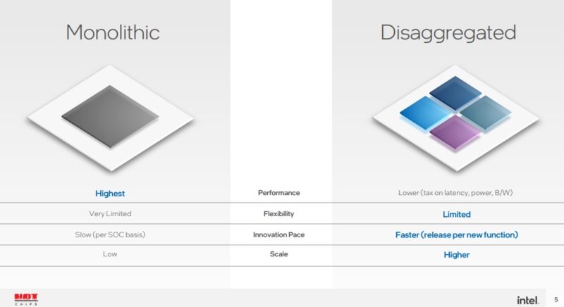
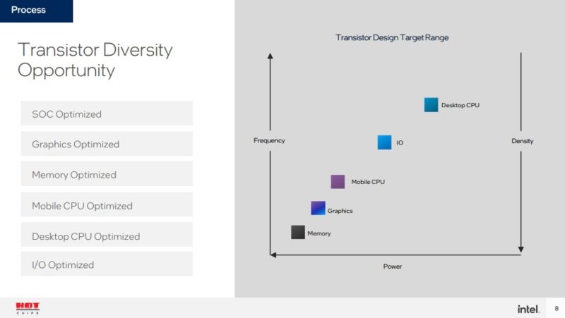
Driving this disaggregation is that different types of transistors are best from a cost/ performance standpoint for certain types of applications. As a result, disaggregation helps to right-size the process for the application.
Disaggregation has been a push for years. This is a relatively lower-end integration than Intel Ponte Vecchio, but is also a higher-volume one.
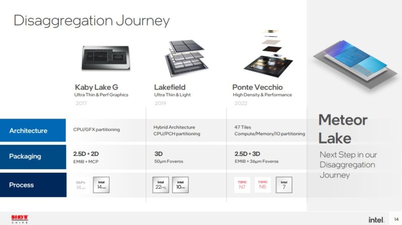
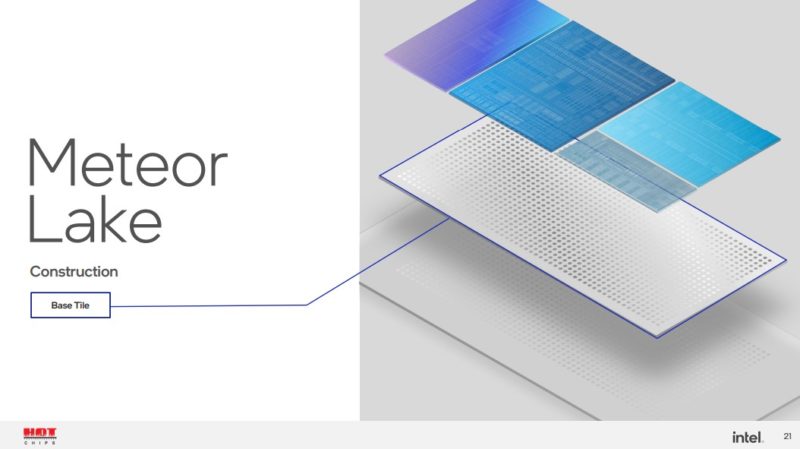
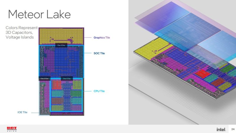
With Meteor Lake, Intel will have a flexible tiled architecture. There will be a base tile and then four tiles that are connected through the base tile to create the package.
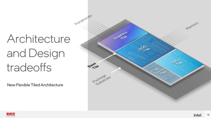
The basic goal is to create a platform that Intel can build upon in pieces.
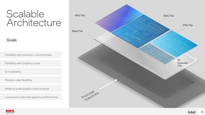
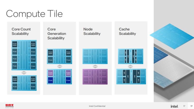
On the compute tile, Intel can scale to different core counts, generations, process nodes, and cache amounts. It can do this without having to touch the rest of the chip. Something worth noting here is that in the above package diagram, the CPU section is nowhere near even half of the package.
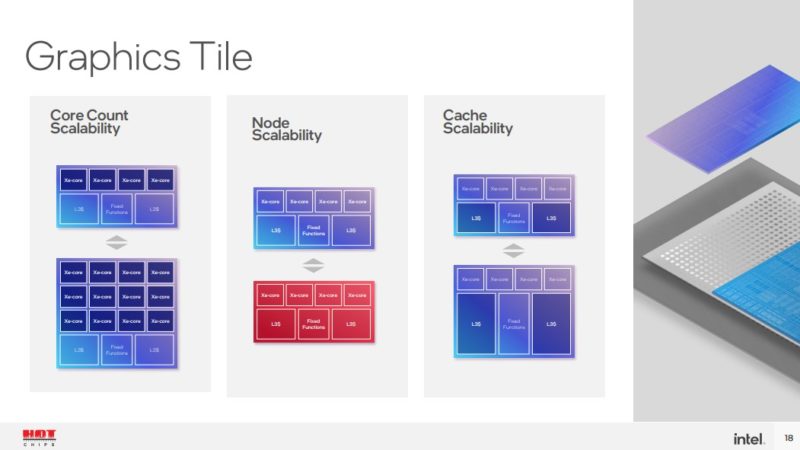
The graphics tile can scale similarly. A note here is that the GPU tile blocks in this diagram are just Xe-cores, caches, and fixed functions. The media and display functions are not here because of the process optimization.
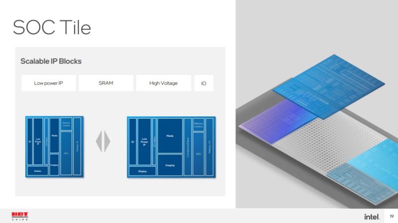
SoC has media display imaging and display (this is not on the GPU tile!) It also has low-power IP, memory control, and more.
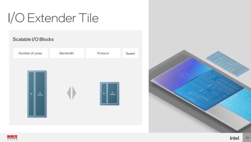
I/O extender tile adds more I/O and that can be varied based on the platform.
Building Meteor lake uses an older generation process as the base die that has the power delivery, I/O and die-to-die wires.
This is what Intel calls a “high yield” process. Part of the new process is having to test individual tiles to have “known good” before assembling. Having a reliable process is important to ensure that the extra assembly steps do not cause issues.
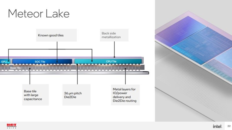
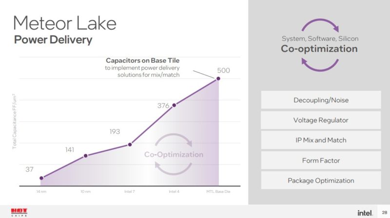
This is the die-to-die and base tile that is modular. Power delivery is a big deal on these multi-chip designs.
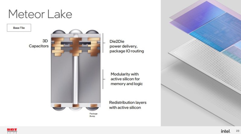
Having different capacitors and voltage islands is important for power but also just integrating different tiles from different processes.
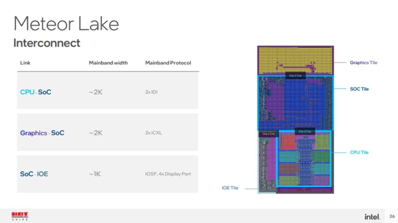
Here are the details on the Meteor Lake Foveros.
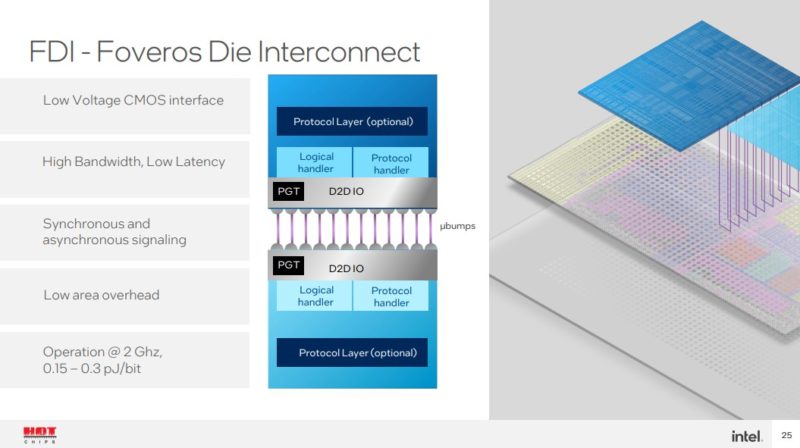
An interesting part of the “iCXL” protocol used by the graphics SoC is that this is a CXL protocol without the PHY.
Creating high-performance products that can scale requires optimizing different processes and packaging for lower thermals.
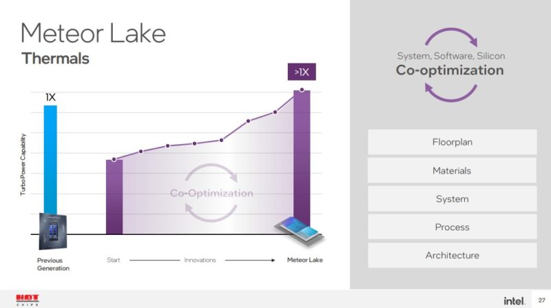
This is more on the importance of the power delivery and capacitors on the base tile.
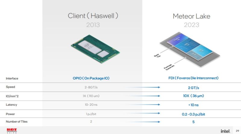
This is a 10-year improvement versus Haswell with an organic package.
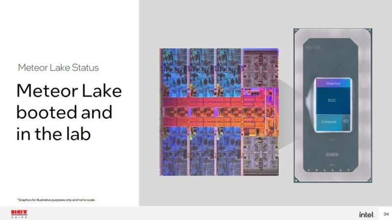
Meteor Lake is slated for 2023 and is already booted in the lab. Intel says that it can manufacture these at scale since these are client devices.
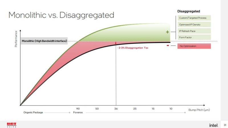
This shows that the “tax” for disaggregation at a 36um bump pitch is only 2-3%. It is hard to even see the different tiles.
With this approach, Intel thinks it can address <10W to 100W+ products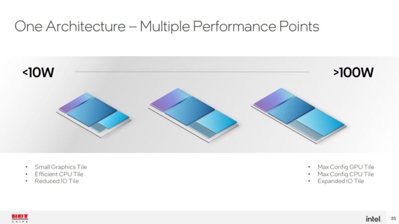
HC34 Intel Meteor Lake Scaling 10W To 100WArrow Lake will swap out some of the tiles to create a new generation of chips. These tiles may be on new process nodes as well. Lunar Lake will have a next-generation 25-micron pitch Foveros.
With this technology, Intel can update portions of the chips without upgrading the entire chip. That means that future mid-cycle refreshes can be more than just 100MHz-200MHz bumps as we had a few years ago. Intel can upgrade cores or the GPU to a new generation without necessarily having to touch the I/O or SoC tiles as an example.
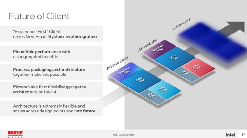
The other implication is that Foveros and Intel 4 will have to be mainstream by 2023.
Final Words
We will get more information on Meteor Lake CPUs in 2023 as the chips launch. There is still some time between now and then. Still, this is an exciting future capability that we will explore more in a second piece later this week. Disaggregated computing is coming to the lower cost consumer segment.


Ah so it begins. The first of the traditional client implementations of CXL. I’m so excited to see what this brings as changes over the next decade in the server and consumer space.
I hope Intel doesn’t segment themselves to death
I am kind of intrigued as to if CXL is more like AGP or more like PCI? As in when we got a new consumer bus interconnect after ISA, AGP had restricted use and sat along side other, more popular slots. Or is it a generational leap for consumer where we’ll have CXL and PCI-E together, then eventually we may get down to one or two legacy PCI-E slots before they eventually disappear?
PCI-e is very ingrained, so it would be bold to remove it completely except for single slot systems. I am not sure I’ve even seen a discussion about the cost of CXL yet? Does the phy and protocol cost more in silicon and IPR? Are there barriers to consumer adoption that aren’t in PCI-e? Is it a battle or are the use cases different enough?
Isn’t CXL using PCIe 5.0 ?
CXL is more like AGP, because it offers additional features over PCIe, but those extra features are not useful for all applications.
For a desktop computer, it would make sense to have 1 or 2 CXL slots, replacing the PCIe slots intended for GPUs, while the rest of the slots remain PCIe.
CXL is useful either for GPUs or other accelerators that may have cache memories, or for memory cards. The latter are mainly useful for servers in data centers, for an extra storage layer between the on-board DRAM and the NVMe SSDs, as explained in other articles on this site.
@AdrianBc
Thanks, that was my feeling, glad someone else views it that way.
This disaggregation of the monolithic die is something they should have pivoted to immediately when they had signs of their 10 nm foundry problems six or seven years ago. Intel was demoing off packaging technologies like this back then and yes while it takes time to go from demo to product, this feels like it is several years late from the potential they had.
There is some understatement in that Intel can do midgeneration refreshes: it doesn’t have to be the CPU die that gets an update. Offering multiple graphics dies or tuning IO to specific markets is also a possibility.
Very excited to see Intel’s segmentation for this. The tile scheme opens entire new dimensions of segmenting.
@Bob H CXL is approx layer 3 or 4 built atop PCIe5’s layer 1 and 2. It is not a replacement, does not specify physical or, afaict, electrical signaling.
Good to see them finally following amd and the rest of the Chip industry
Another coverage mentioned that the GPU is connected by 2K foveros connections. Looks like their iCXL is CXL protocol over a wide parallel interconnect with the lower clock speed 2GT clock rate. Was Intel explicit about this?
While on one hand this Starbucks type chip personalization sounds super nice (actually it just bring back some of the flexibility that PCs with slots used to have), what’s missing is instant delivery with the notebook or whatever form factor of your choice. Well these days with the chips pandemic people might actually find weeks acceptable, but the just the production pipelines on these chips are more likely to run for months, just for the SoC, while product cycles may not be longer.
What I see coming, is a worsening of SKU hell. Companies like Lenovo are already permutating just about every form factor, design line (plastic/metal), screen type (touch/normal/gamer/OLED*resolution), CPU class(i3-9*vendor) and they need to produce at scale based on plans they can turn out rather ill matched due to whatever.
So while the base might allow for near infinite variability they are more likely to stick to few volume items which negate much of this flexibility, because they don’t want to wind up with inventory they’ll have to dump. I guess it’s one of the reasons nobody wants to sell me ultrabooks with 64GB of soldered RAM: while it’s a ‘penny expense’ for the RAM, you only ever get to choose between 8 and 16GB unless you go ’boutique’.
While I’d sure like to be able to assemble my dream SoC from these various Lego tiles and put it into the various shells I’d customize the same, I don’t see just-in-time manufacturing coming to <€999 ultrabooks and neither swappable SoCs when batteries are glued, so Intel may be overestimating the potential and appeal quite a bit.
Comments are closed.