
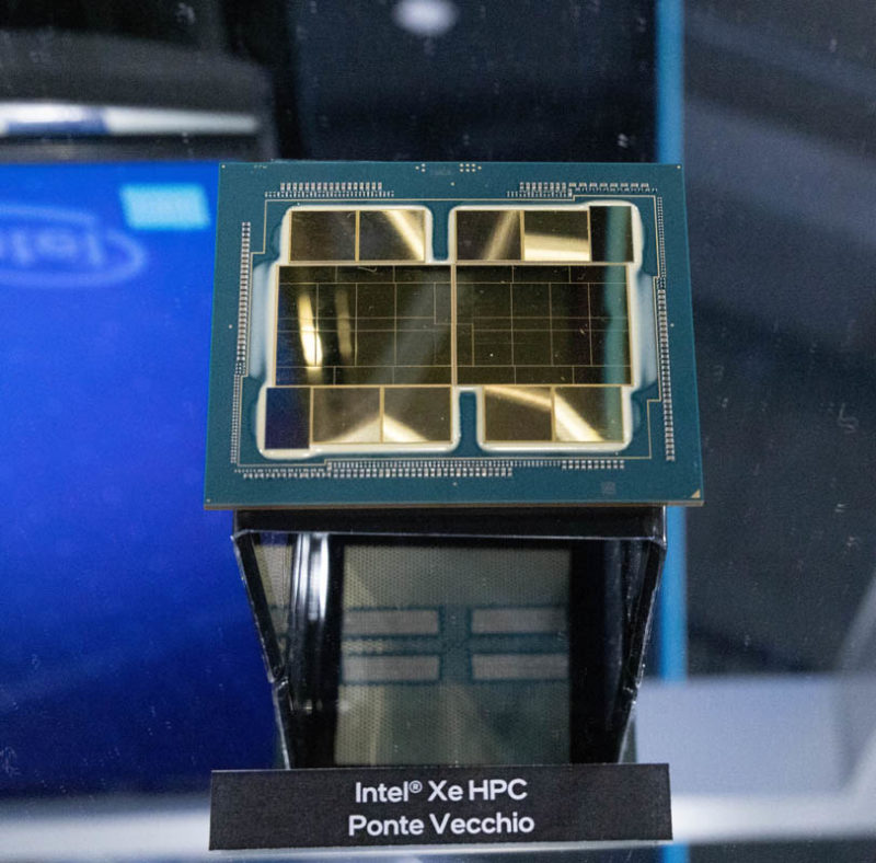
At Intel’s Vision 2022 event, we were able to check out the Intel Ponte Vecchio GPU and it is as impressive in person as in renderings. There is a ton of silicon onboard, and this is what we have called a spaceship of packaging technology. Intel is packaging tiles from multiple fabs and on different processes together to built the Xe HPC GPU.
Intel Ponte Vecchio GPU Packages at Vision 2022
Here is a look at the package from the top. One can see all of the tiles clearly which was very interesting. The package part is larger than the NVIDIA H100. We have photos of the H100 SXM5 module, but the silicon part of the NVIDIA package is smaller. Although we held that part of the NVIDIA competition, we were not able to take a photo of it.
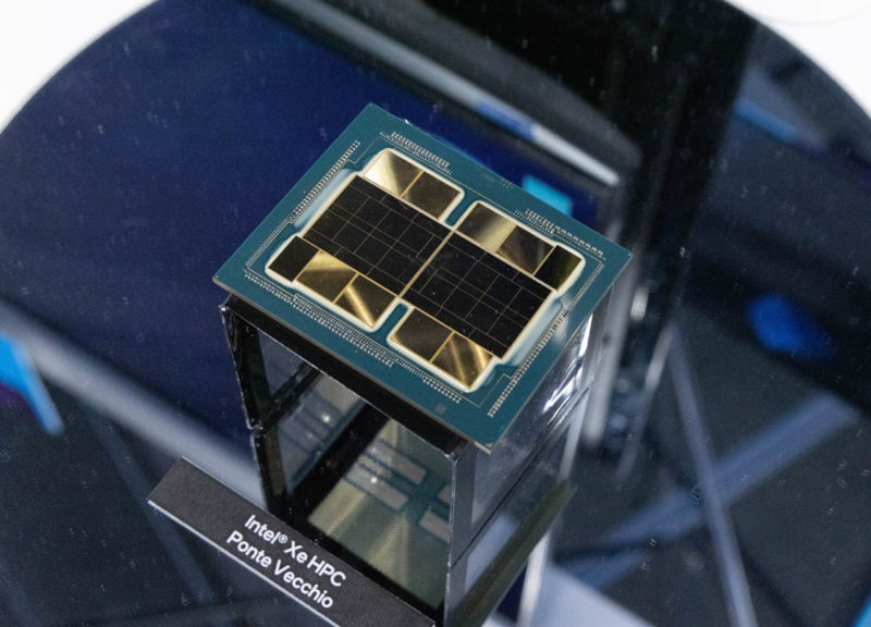
Here is the new Intel Xe HPC GPU from another angle:
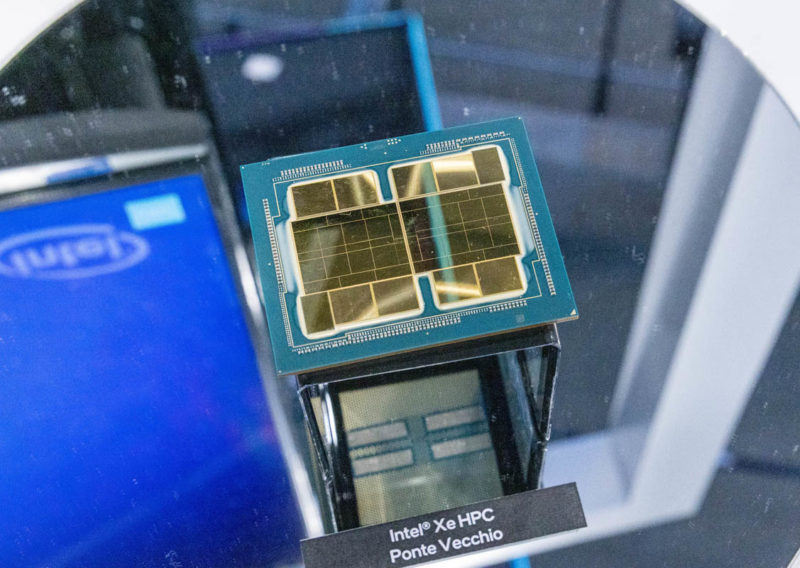
Here is yet another angle with a bit different exposure where one can clearly see the tiles.
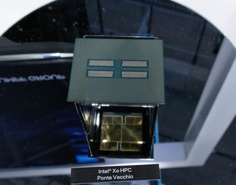
Something that does not get mentioned enough is the bottom side. Intel has a large number of pins below the package.
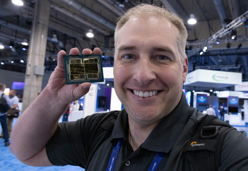
We also have a silly face cover image for this one:
Overall it was great to see the new GPUs on the show floor.
Final Words
Many of this year’s Ponte Vecchio GPUs will be going to the Argonne National Lab for its Aurora supercomputer. We will have more on that post-event. In the meantime, feel free to check out our Intel Ponte Vecchio is a Spaceship of a GPU piece, the Hot Chips 31 piece, or this video to learn more:
This is a very exciting product in the industry aiming to be a competitor to the NVIDIA H100. It is also the start of Raja Koduri’s 1000x in 5 years Zettascale computing plan we discussed Raja’s Chip Notes Lay Out Inte’s Path to Zettascale.
Just a few fun videos for you to check out.


Surely space station instead of space ship?
Given the larger number of chiplets, what is the assembly yield loss?
Who is doing the package assembly and where?
Has Intel already shipped the 60,000 Ponte Vecchio to Argonne National Labs?
Comments are closed.