
Today’s big announcement is the Universal Chiplet Interconnect Express (or UCIe) industry effort. UCIe 1.0 is designed to allow silicon providers to focus on building best-of-breed silicon IP, then having the ability to package these chiplets together. We have been discussing some of the early mentions of these efforts at STH for some time, but now we get to put a name to it.
Universal Chiplet Interconnect Express UCIe 1.0 Launched
As a bit of background here, companies that sell and consume systems need a way to customize chips for unique workloads. The chip industry has become so large that having a small number of monolithic dies servicing all segments does not work. Furthermore, there is now enough worldwide volume to allow more specialization.
A great example of this is the difference between HPC clusters, network firewalls, and web servers. HPC servers need parallel double-precision floating-point processing and high memory bandwidth. Network firewalls need cryptographic offloads, packet processing acceleration, and network interfaces. Web servers can get by with many cores and mostly focus on integer performance while needing to scale core counts. All of these chips are fundamentally different and will have different power, cooling, and networking needs.
Chiplets provide the path to integrate IP blocks that serve various functions and then package them according to an application. When we hear Intel discuss its plans for its Intel Foundry Services (IFS) and how it plans to help customers, this is exactly why. Intel’s packaging technology allows it to not just manufacture its own chips, but also take chips from other foundries and integrate them into solutions, adding value atop of the entire stack by providing the packaging. If you read our Intel Ponte Vecchio is a Spaceship of a GPU piece, this is perhaps the biggest impact here. Intel is getting into multi-fab packaging, and Ponte Vecchio is a packaging showcase.
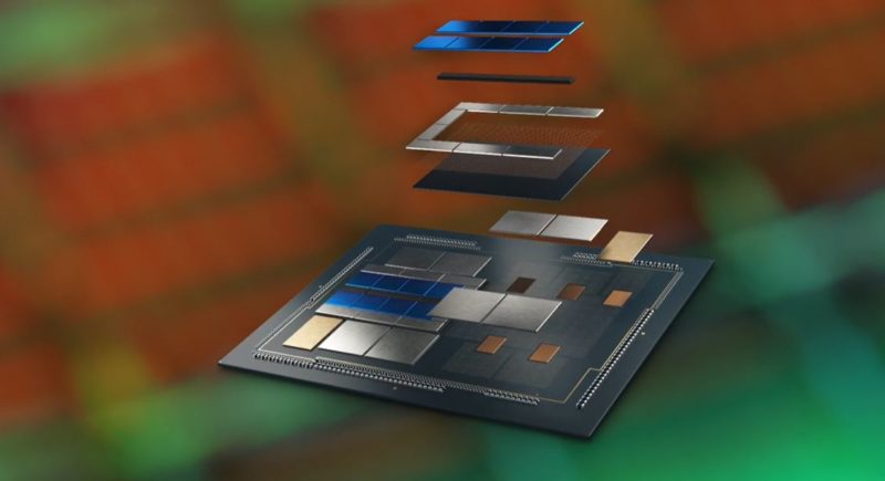
AMD for its part has been packaging TSMC compute dies with Global Foundries I/O dies for years and we expect to see more complex packaging in the future. Although we have been discussing Intel a lot here, before we get too far into this, it is worth looking at the promoters:
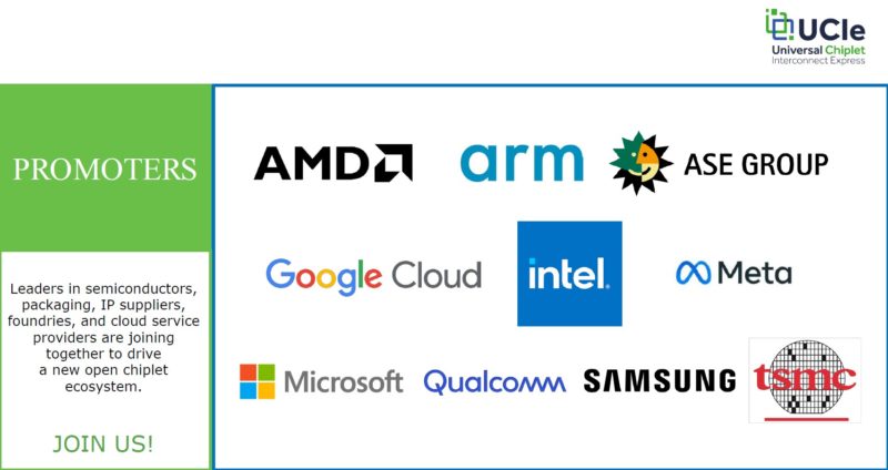
We have the four major hyper-scalers in the US, aside from AWS. We also have many of the world largest chip IP vendors. This is going to happen because big customers want it, and big chip companies are going to provide it. Getting back to the customization aspect, the cloud players may eventually decide to do things like integrating networking or even DPU-like features into chips to streamline their architectures. Since these large players make up such a large piece of the ecosystem, they want specialized chips that cater to their needs.
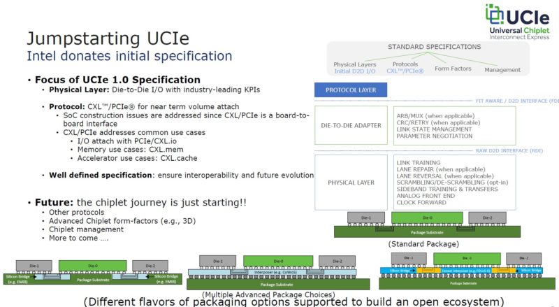
Saying that companies want to integrate is great, however, desire alone does not make chips. Instead, to get IP from different companies there needs to be some set of standards to allow this to happen. UCIe is that standards effort.
This concept we have actually discussed before. In my discussion with Raja Koduri at Intel (see Raja’s Chip Notes) we discussed Lightbender Silicon photonics chiplets that will come in the Falcon Shores era for supercomputers. Raja’s key insight was that one of the biggest challenges with integrating Silicon photonics at Intel has been getting it into monolithic dies. By instead specing a set of interface and power parameters, Intel could have a chip that would fit in a certain size and power envelope (I am probably not supposed to talk about the power, but it makes a lot of sense), and with a set of interfaces, it basically makes future chip building like building software with API’s then building chips with the API’s provided by different teams. Another software way to think about it is like silicon containerization.
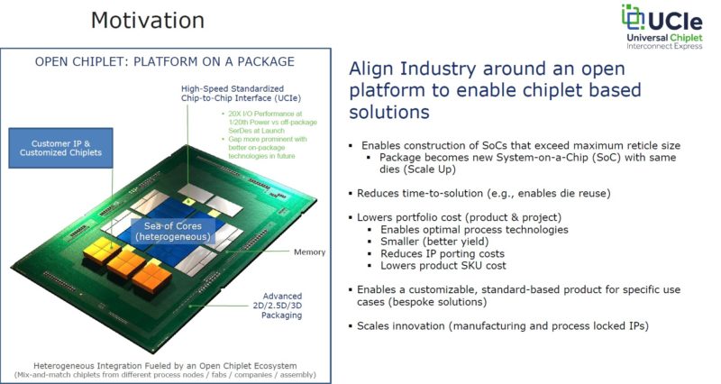
At the heart of UCIe are some well-known technologies such as PCIe and CXL. This allows chiplets to interface in a common way and transition from external devices to chiplets. UCIe also addresses things like how chiplets are packaged. Of course, in the future, we will see more standardization on things like form factors. After all, a chiplet design becomes more powerful if one can swap new generations of technologies from different vendors as needed. This is just like PCIe cards, OCP NICs, SSDs, and more have standard form factors.
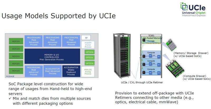
When one looks at the usage models for UCIe, it becomes clear what is happening here. Many of the items that used to be add-on boards or devices are going to be packaged together.
The best way I can draw an analogy here is just thinking back to computers of years past. Many of us remember the late 1990’s and early 2000’s when a desktop computer would have a motherboard. There would then be external caches, memory, drives, network cards, GPUs, sound cards, storage adapters, and so forth. If you have seen our TinyMiniMicro series looking at 1L corporate desktop PCs, then you will see systems without these cards sticking out from a large motherboard. Over time, common features get absorbed into larger packages. At the same time, that integration means the amount of connectors on motherboards or those 1L PCs has gone up and that is why adding off-package connectivity is important. Remember, Intel Lightbender will have the ability to reach off-package and connect things like stacks of memory or other chips so Intel needs this capability.
The bottom line is that this needs to happen in the industry. While companies are talking about handheld devices, perhaps the big driving force these days is in servers. The large cloud providers want to customize silicon for specific roles in their infrastructure.
Final Words
Looking ahead, it will impact the way we purchase servers and other devices in the future. Having a Lenovo or a HPE Intel Xeon may be different in the future. Folks have been very charged about Lenovo Vendor Locking Ryzen CPUs with AMD PSB, and both Dell and Lenovo doing the same on servers. Chiplets offer a path for fully locking packages and functionalities to certain systems, and creating either more or less interoperability between vendors’ solutions. To us, the one aspect that needs to be clearly addressed in this is defining models for reusability since that circular economy piece has the ability to create or divert large amounts of e-waste.
Overall UCIe is a step into the chiplet world that is needed. There is still work to do, but having standards is important. Not only will it shift how chips are designed, but it will also shift the value chain for those providing, IP, foundry, and packaging services. One of the exciting developments here is that we are nearing an era with many more chip designs than the era we are exiting.


Now we will need tweezers to swap our GPU! Still, it is progress.
I could see some use cases beyond servers, but the problem is the volumes involved. Since STH is focused on the USFF/Tiny/1L form factors, I could see a chiplet design that incorporates the cores, the memory and then some features that very desirable in the world of USFF.
High performance storage chiplet controller, a high speed networking chiplet controller(s) and a choice of other technologies to speed up other processes like a Risc-V/ARM chiplet. Just examples.
If the flexibility of fabbing these chiplets holds up, you could technically order a chiplet combo of your choice (build to order) as long as they have a supplier of like design chiplets to include in the overall package. Naturally this will require a socket that can support all of these leads this approach can support.
In the real world, the OEM’s will not be this flexible as they will require lowest cost and that means the same thing made several million times. Those type of supply deals require long lead times and lots of demand forecasting.
But I do see a niche forming where someone (like a Hardkernel or Minisforum) uses capacity at one of Intel’s custom fab arrangements to integrate a chiplet combo and therefore distinguish themselves in the SBC or mini market.
Comments are closed.