
Years ago we had a great NVIDIA NVSwitch Details talk at Hot Chips 30. With Hot Chips 34, we get the H100’s NVLink4 generation. In the talk, NVIDIA discussed more about NVSwitch and NVLink4 that it uses to provide a communication fabric for its GPUs.
Note: We are doing this piece live at HC34 during the presentation so please excuse typos.
NVIDIA NVLink4 NVSwitch at Hot Chips 34
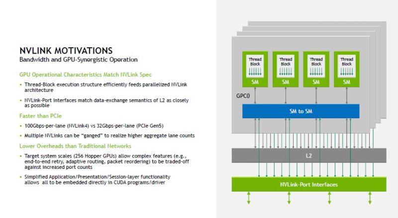
NVLink is born out of two needs from NVIDIA. One, it needs its GPUs to have the highest performance possible. Second, having a proprietary interconnect allows it to dictate systems design in order to achieve that higher performance. As an example, NVLink is 100Gbps per lane while PCIe Gen5 is only 32Gbps per lane and NVIDIA uses multiple lanes to connect its GPUs.
At the start of the talk, NVIDIA showed NVLink Generations. We have used every version of NVLink 1-3. With the P100 generation we had content like How to Install NVIDIA Tesla SXM2 GPUs in DeepLearning12, V100 we had a unique 8x NVIDIA Tesla V100 server, and the A100 versions as well.
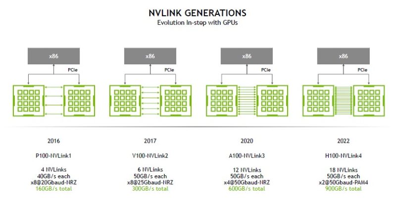
With the H100 generation, we get the 50Gbaud PAM4 but we scale from 12 links to 18 links. That gives 50% more bandwidth. Here is what the topology looks like with this generation. A few notes:
- The P100-NVLink1 generation did not use NVSwitch in the DGX-1
- With the V100, we got the V100-NVLink2 with the DGX-2 to support the larger number of GPUs
- A100-NVLink3 is where in the DGX A100 NVIDIA doubled bandwidth.
- With the H100-NVLink4 NVIDIA is focused more on scale-out with NVLink.
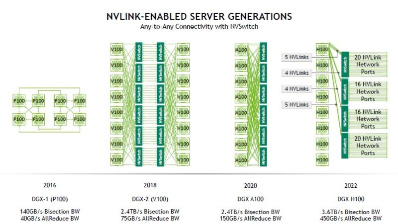
One of the big benefits of transitioning to NVLink4, aside from bandwidth, is that one can use fewer NVSwitches to support the same number of GPUs.
Here is the shot of the NVLink switch where around half of the switch chip is dedicated to PHYs. This is a TSMC 4N process and uses 1/3rd to 1/4th the transistors of a modern GPU.
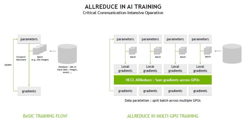
One of the big features is AllReduce acceleration using NCCL.
Here is a look at the traditional calculation:
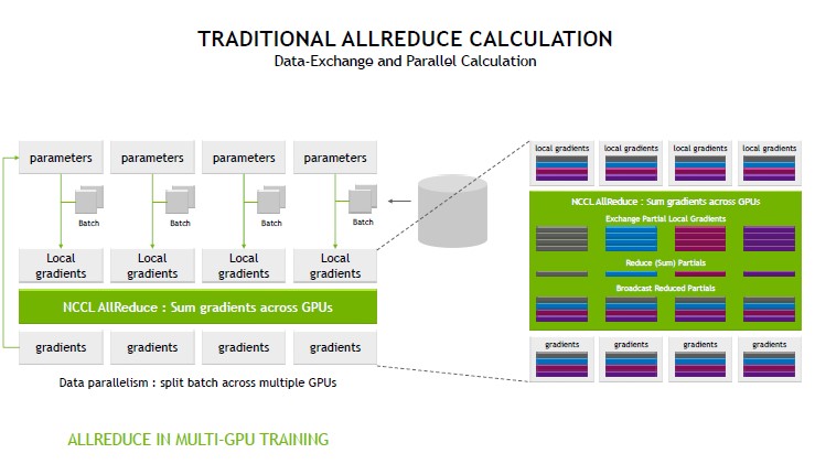
What NVIDIA basically does is that instead of having to collect everything, then send out results, it is able to perform this calculation in the switch chip and then update. The benefit here is that it is not over computationally taxing, but it reduces network traffic. This in turn increases performance by eliminating a lot of network traffic to get a simple calculation done.
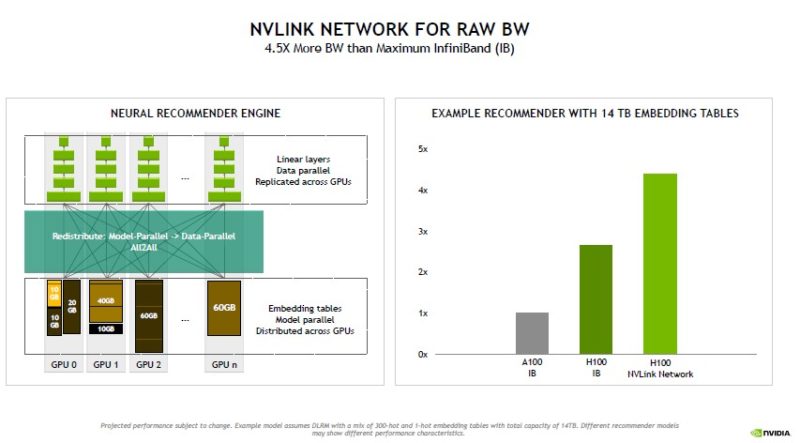
For raw bandwidth, NVLink is faster than InfiniBand, NVIDIA’s scale-out interconnect.
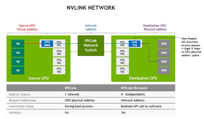
Hopper and NVLink4 build more on the security and functionality standpoint as well.
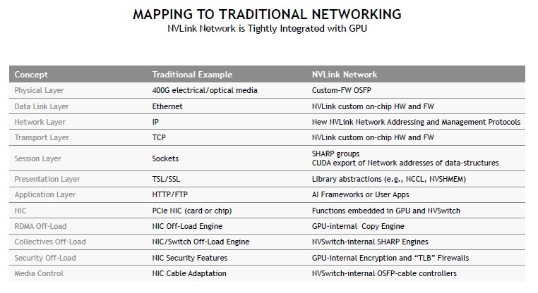
Here is a mapping to traditional Ethernet networks and what NVIDIA customizes with NVLink.
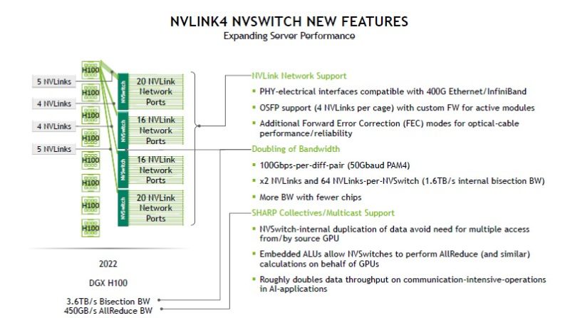
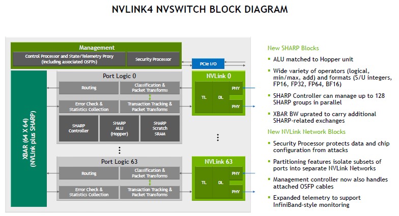
Here is the NVLink4 NVSwitch Block Diagram with the new SHARP blocks is below. The key is also that NVIDIA owns CUDA so it has the software side to integrate these different components like SHARP blocks.
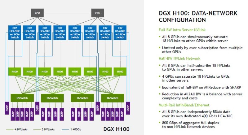
Here is a look at the NVIDIA DGX H100. We highlighted the NVIDIA Cedar Fever 1.6Tbps Modules Used in the DGX H100 already so these are not separate PCIe cards like the BlueField-2 DPUs that sit inside a DGX H100 but are not on this chart.
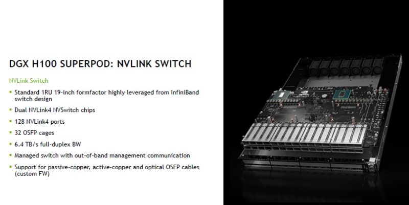
This is the 1U DGX H100 SuperPOD NVLink Switch. We can see two NVLink4 NVSwitch chips onboard.
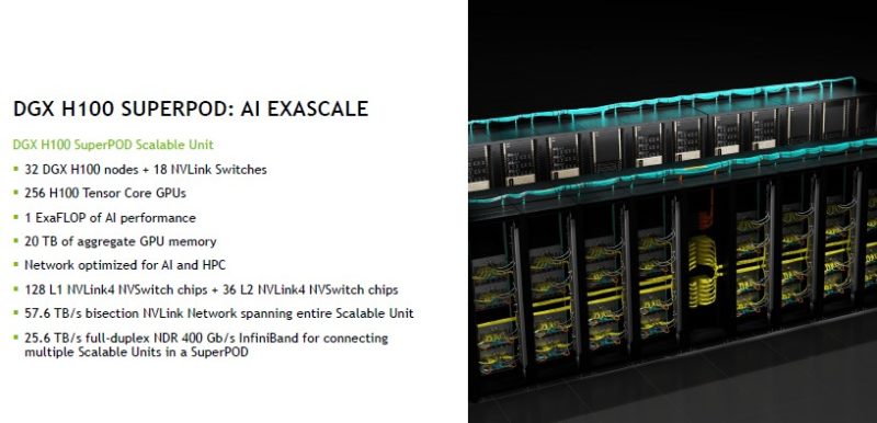
NVIDIA has the DGX H100 SupePOD with 32x DGX H100 nodes, 256GPUs, and 18 NVLink Switches here.
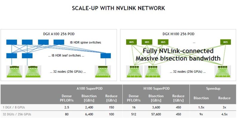
Being able to scale up to 256 GPUs in this NVLink generation means NVIDIA can connect more GPUs without having to go over InfiniBand.
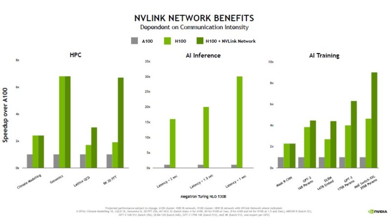
Here are the claimed network performance benefits.
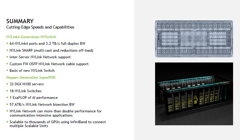
This is the summary slide with details we have already seen.
NVIDIA has some interesting technology because not only is there NVLink but then going to larger clusters and to storage the company has InfiniBand and Ethernet.
Final Words
When the HC30 NVSwitch presentation happened, NVSwitch was new and super exciting. We had not gotten hands-on with the DGX-2. Now, the NVSwitch is a better-known quantity and we are seeing a natural progression of the technology. The big difference these days is that NVIDIA is going beyond the chassis and looking at integrating NVSwitch to multiple chassis and systems that would have previously only been connected via InfiniBand.


SHARP is an IB technology. Does its inclusion in NvSwitch imply there is IB support embedded in NvLink now? Or did Nvidia port the technology into NvLink without the IB protocol somehow?
The NVswitch stuff is probably where NVidia is the most advanced compared to the others. Very cool stuff.
I wonder how much SRAM there is on chip though. Must be pretty hard to schedule the reductions of GBs of data with just on chip SRAM. Wouldn’t be surprised if the next gen has its own HBM/LPDDR.
Comments are closed.