
At STH, we have our first DGX-1 (or DGX-1.5 if you want) class machines in the lab. The NVIDIA DGX-2 is the next step up with up to 16x Tesla V100 GPUs. The DGX-2 architecture is underpinned by the NVSwitch chip which makes the entire machine work and provides a significant architectural benefit. At Hot Chips 30, the company disclosed more information about the NVSwitch. We have a companion piece around the NVIDIA DGX-2 details the company released.
NVIDIA DGX-2 and NVSwitch Context
The NVIDIA DGX-2 utilizes 16x NVIDIA Tesla V100 GPUs with up to 32GB of memory to create a massive GPU compute machine. Since the NVIDIA Tesla V100 is already near the limits of a practical GPU chip, scaling means distributing work over more GPUs. The DGX-2 uses NVSwitch chips to stitch GPUs together and create a 16x GPU system.
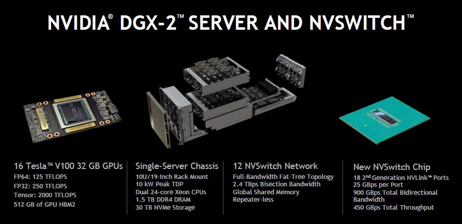
NVIDIA’s goal is to effectively create a “single” GPU that can scale up to handle larger problem sizes.
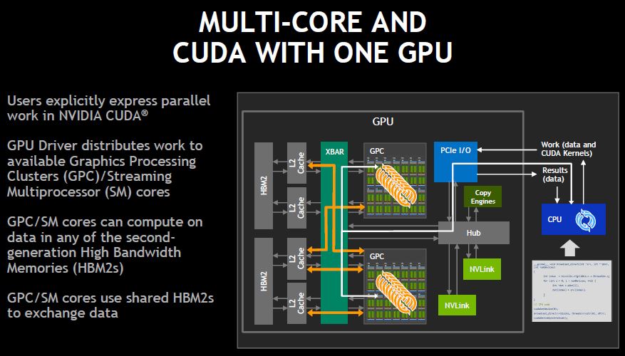
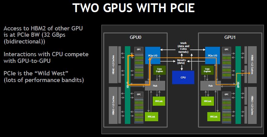
In DeepLearning10 and DeepLearning11 we explored scaling GPUs over PCIe. One of the issues there is that the GPUs have to communicate over PCIe which has limited bandwidth.
Using NVLink between GPUs allows faster access between GPUs by bypassing the PCIe bus. It also moves GPU-to-GPU communication off the PCIe bus where traffic from Infiniband/ Ethernet cards and storage resides.
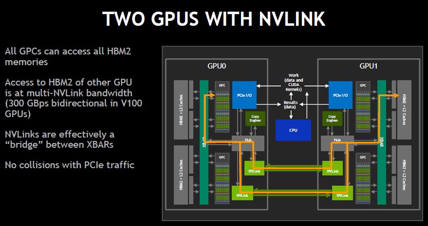
Using NVSwitch and NVLink, NVIDIA DGX-2 is designed to be one gigantic GPU since there is a high-speed, low-latency interconnect, GPUs can access HBM2 memory of other GPUs instead of having to go back to main memory.
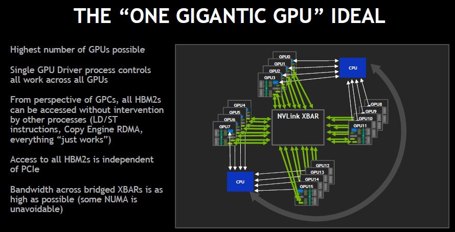
The net impact is the ability to load data into the HBM2 memory and treat it as a single GPU.
Digging into the NVIDIA NVSwitch
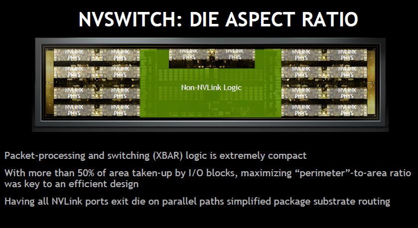
At Hot Chips 30, NVIDIA gave more details about the NVswitch. One of the first points is that the NVSwitch is fabbed on the same TSMC 12FFN process as the NVIDIA Tesla V100. That means the company can re-use the NVLink IP blocks.
That shape is a long thin rectangle. This is to maximize the amount of I/O and make traces between switches and GPUs easier. NVIDIA declined to give power figures, however, it says the PHY is lower power because it is built on 12nm.
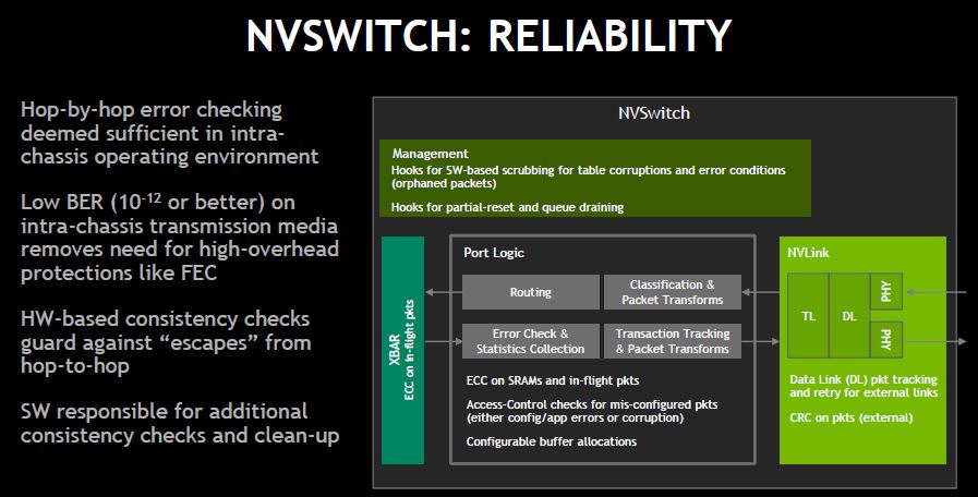
The primary mission of the NVSwitch is to bridge GPU XBARs between multiple GPUs. It has a non-blocking XBAR. The NVSwitch packet transforms are spoofing messaging to make responses from all of the other GPUs look like one stream to a GPU since NVLink assumes GPU to GPU communication.
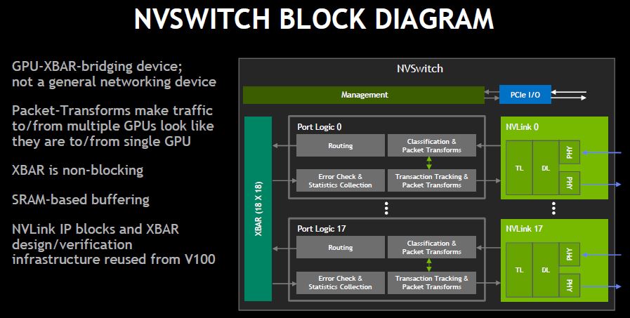
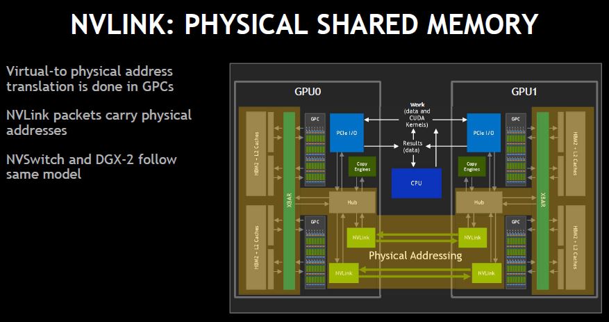
NVLink uses physical addresses everywhere. One of the functions of NVSwitch is to take all of the GPU address space and turn it into a global address space.
Since it is designed to be in a single chassis, the in-chassis transmission is extremely reliable. As a result, NVIDIA does not need forward error correction and other expensive error correction mechanisms.
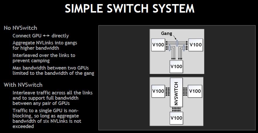
Without NVSwitch, you can only get half of the bandwidth in “gangs” between Tesla V100 GPUs (P100’s had fewer NVLinks.) The NVSwitch allows full bandwidth to each GPU.
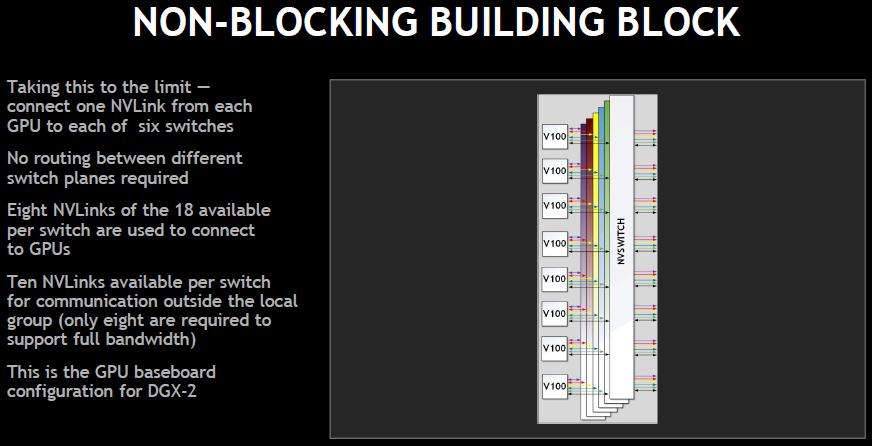
Since each GPU has six links, it can go to six NVSwitches. Each switch uses less than half of the ports for GPUs.
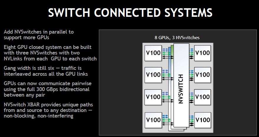
The aggregate HBM2 bandwidth of the machine is 14.4Tbps and the switches are non-blocking.
Final Words
Overall, this the “secret sauce” to the NVIDIA DGX-2. The big question is how much power these chips use. If you look at the power consumption between DGX-1 and DGX-2, the DGX-2 does not have twice the CPUs and adds NVSwitches. At the same time, it uses more than twice the power. Check out our NVIDIA DGX-2 article for more on that system.


