NVIDIA A40 Performance
In terms of performance, the NVIDIA A40 has been out for quite some time at this point, but we just wanted to show a different view than is publicly out there using multi-GPU systems. We noticed slight variances between either GPUs, or GPUs in the larger 8x and 10x GPU systems that we reviewed such as the ASUS ESC8000A-E11.
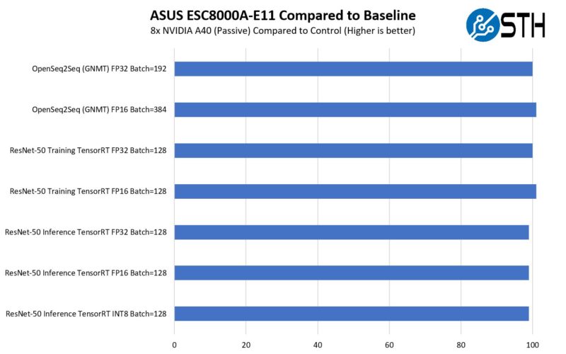
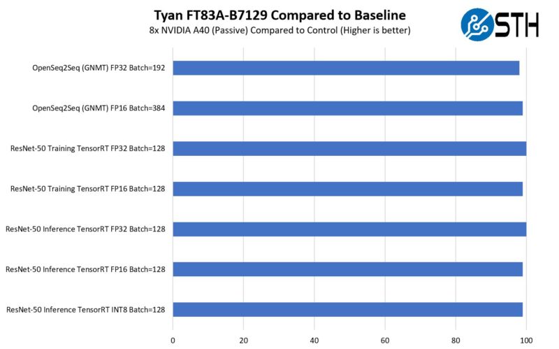
Also, the Tyan Thunder HX FT83A-B7129 saw variances across our quick deep learning benchmarks.
In terms of performance, this is a rough guide, but a PCIe NVIDIA A100 doing training will be around twice as fast, and the top-end SXM4 80GB 500W A100’s as we tested in Liquid Cooling Next-Gen Servers Getting Hands-on with 3 Options are roughly about 2.4-2.5x as fast with something smaller like ResNet-50 training but that delta can go up as one uses more memory and NVLINK with larger models.
Still, the real reason one uses NVIDIA A40’s is not necessarily for the training performance. Instead, they tend to sell for much less than a NVIDIA A100 SXM4 solution, while at the same time providing vGPU features for solutions such as VDI/ virtual workstations.
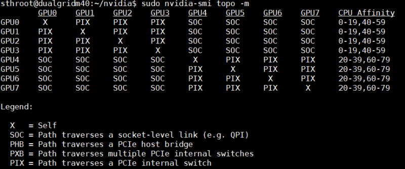
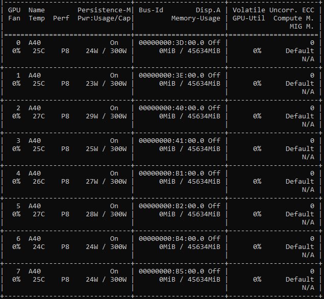
While we did not have NVLINK bridges, here is what eight of these GPUs look like in an AMD EPYC system without PCIe switches. As we can see, we simply have an 8x PCIe link topology.
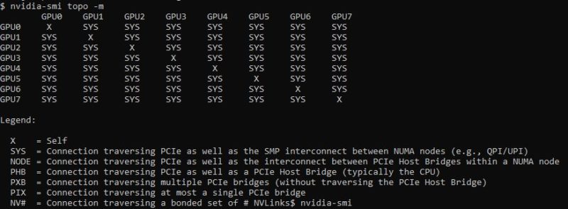
This is certainly different from the NVIDIA M40‘s that had four GPUs per card from a few generations prior. Here are eight M40 GPUs, using two M40 PCIe cards (four GPUs per card):
One of the great things is that there is no longer a need for a more complex PCIe architecture for a VDI card like this.
Next, let us get to power consumption before getting to our final words.
NVIDIA A40 Power Consumption
The power consumption of NVIDIA’s data center GPUs tends to be very different from Intel CPUs, and sometimes AMD CPUs. Specifically, the cards have a power cap and if you run them at their maximum, they will effectively try to hit their caps (you can also use nvidia-smi to set lower caps for lower power/ performance operation.) So saying that these consume 296-300W at 100% utilization is very safe. Instead, we wanted to show the idle power consumption of the 16x units we had in two different servers. As passively cooled cards, these do not have fans to spin up, so the idle is just for the compute resources. Here is one set:
Here is another.
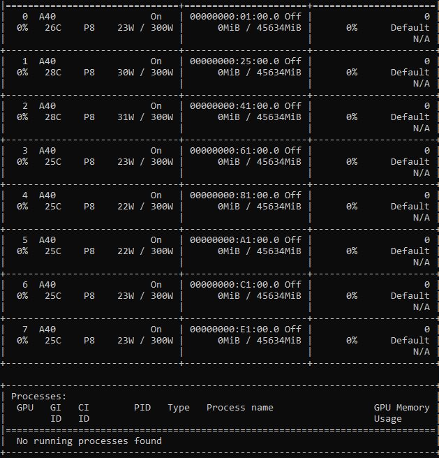
Based on this, we have roughly 25-31W at idle for the sixteen different GPUs. That is only part of the equation though. Between power supplies and fans used, there can be 20%+ power used in a system due to the chassis fans running to cool the GPUs. We had a piece where we investigated several factors that impact server power consumption.
An important aspect when adding a NVIDIA A40 to a system is that the GPU itself uses 300W, but in the context of an overall system, it can easily add 360-400W of power draw at the PDU depending on the server’s power supply efficiency as well as the cooling. Given how much power is being consumed by cooling, many next-gen systems, and even A100 systems are turning to liquid cooling, and that is why we have been focusing on that recently.
Final Words
If you are looking for a NVIDIA GPU to do VDI workloads, then this is really the top option for the data center where one can handle passive cooling. 48GB is a lot of memory to split among VMs. The NVIDIA A40 is an Ampere part, but realistically, higher-end training will have folks look to the NVIDIA A100’s with NVLINK. The other side is that the capable GPUs can handle VDI workloads during the day, then use the GPUs for GPU compute in the evening.
For our regular readers wondering, yes, this was done just before GTC 2022 as we had a few backlog items to get through before then.


 and show some of its interesting features)
This GPU is rated 0.5 TFlops double precision with single precision an astonishing 64 times faster than double.
For reference a lowly Radeon VII yields 3.3 TFlops of double precision which is about 6 times faster than the A40.
In my opinion the level of market segmentation that Nvidia is practicing with their GPUs right now can’t be good for anyone but Nvidia.
Since the main advantage GPGPU computing has over special-purpose neural network hardware is that GP stands for general purpose, it would be useful to test a comprehensive selection of general application domains in the GPU reviews. Such tests are especially important for GPUs with intentionally lopsided capabilities that target very specific market segments.
What your pair of bar charts are supposed to mean?
Are you comparing the A40 cards on hand to past A40s you’ve tested? Are you comparing the same cards running in different servers (ie the charts are actually server comparisons?)
Anyway, A40 (A10, A6000) have negligible FP64 ability but superior FP32. A100 is an FP64 monster with relatively modest FP32.
Ironically, you seem to think you are complaining about too much market segmentation but in fact you are complaining about not enough. Additionally, more segmentation of the type you are looking for would result in more expensive parts, or simply the market not being served at all. Most GPU domains do not require FP64 operations. The A40 is based on the GA102 GPU which is the top-of-the-line graphics/gaming oriented GPU from NVIDIA. By including full FP64 on it, it would lose performance in its core markets: gaming and professional graphics. If you want FP64 on a data center NVIDIA GPU less powerful than an A100 then you have to go for the A30 or for an older generation Gx100 GPU. If you want both ray tracing and full FP64 on the same GPU then you must either go to another manufacturer or convince NVIDIA that the size of your market is large enough to either 1) warrant NVIDIA spending hundreds of millions of dollars to make a special GPU for the market or 2) warrant NVIDIA spending money to add ray tracing to all data center GPUs and reducing the CUDA performance somewhat in the process due to the loss of die area and sacrifices that must be made to optimize for a greater set of constraints.
@Matt I don’t think OP was thinking that FP64 uses dedicated silicon, and I don’t think so either. In the earlier days of Quadro (think Kepler) the Titan used the same chip, but had FP64 cut by 2/3.
@steffen It does use dedicated silicon as NVIDIA architects it now. If I remember, in Kepler FP64 also used dedicated silicon. They cut the FP64 rate in firmware for differentiation purposes, as did AMD. In the Tesla (architecture, not product line) generation, and maybe in Fermi, NVIDIA had FP32 units built into their FP64 units and so didn’t use as much extra die area for the FP64. However, I believe that’s less energy efficient and that’s why they changed it. Or perhaps they changed it for some other reason, such as easier optimization or ability to reach higher clock speeds. Regardless, AMD followed suit. Also, the fact that AMD produced the Radeon VII (in extremely low quantities) has no bearing on the fundamental physics. AMD was looking for markets for chips. The card sucked for most use cases and, as noted, was produced in very low quantities. If anything it can be used as evidence that use case differentiation in the GPU space is very real. There’s so much “conspiracy theory” online when it comes to Nvidia. It’s tiresome.
Comments are closed.