
Today we are going to take a quick look at the NVIDIA A40 GPU. The A40 is a 48GB GPU that is passively cooled, yet also has video outputs making it a very interesting card. Furthermore, it has a 300W TDP making it a PCIe Gen4 GPU with a relatively high TDP that can be used in professional workstations and servers. We have already seen the A40 in a number of STH system reviews, but today, we decided it was time to give the unit its own piece.
NVIDIA A40 48GB GPU Hardware Overview
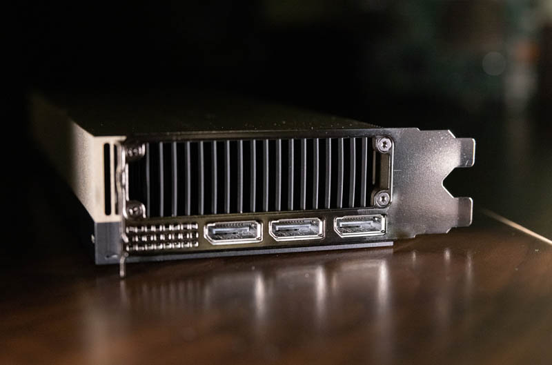
The A40 card itself is a double-width full-height full-length PCIe Gen4 GPU. This uses NVIDIA’s gold theme and looks similar to many of the other NVIDIA PCIe GPUs of this generation that we have used.
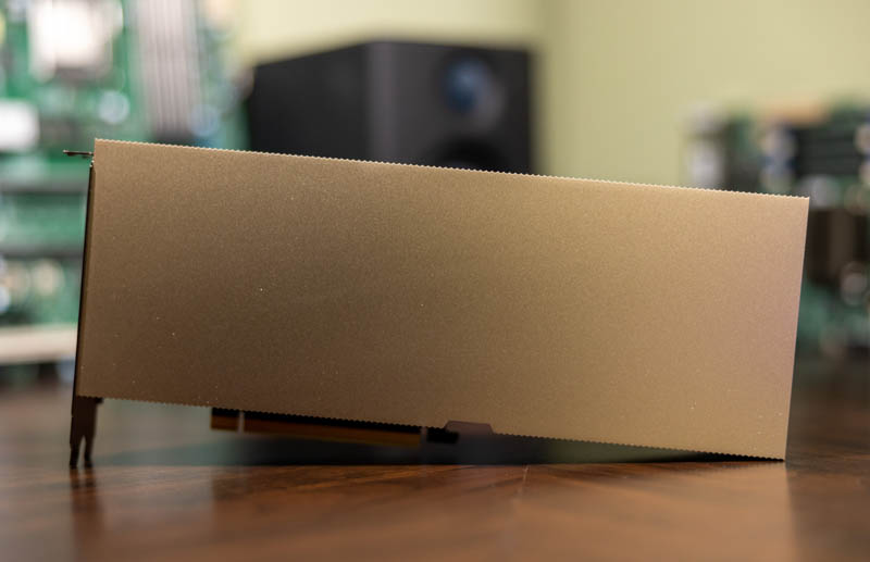
As we expect, this is a newer PCIe Gen4 generation GPU, so it is likely to be paired with 3rd Generation Intel Xeon Scalable “Ice Lake” or AMD EPYC 7002 “Rome” or EPYC 7003 “Milan” CPUs. We still get a standard PCIe Gen4 x16 edge connector on the card.
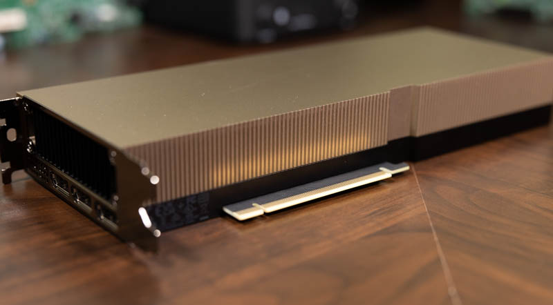
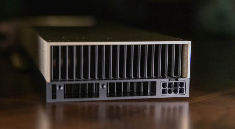
Cooling on the GPU is passive, but NVIDIA says that the card is able to handle airflow in either direction so air can be pushed or pulled through the heatsink. As some frame of reference, the GPU with its PCIe I/O plate is around 1kg/ 2.2lbs so the heatsink has significant heft. We also get a standard 8-pin data center GPU power connector on the rear of the unit. That section also includes holes for vendor-specific mounting support brackets.
On the top of the unit, we get something that is fairly interesting in that we get a NVLINK connector. We did not have the bridge for this one when we had multiple A40’s but the feature is present.
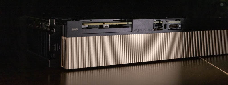
On the I/O faceplate of the unit, we get three display outputs. These outputs are actually disabled by default. NVIDIA does this so SR-IOV support works out-of-the-box for NVIDIA Virtual GPU software, such as the editions used for VDI. One can also enable the display outputs for other software configurations and can also span multiple A40 cards for display using Quadro Sync II.
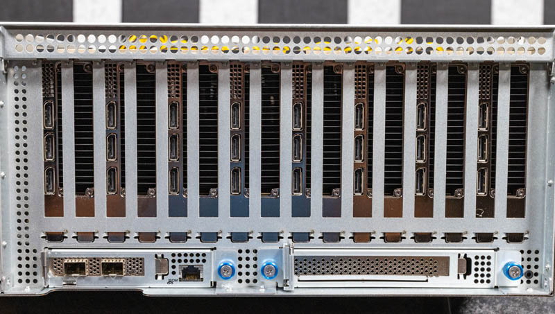
This is a big deal since we can get SR-IOV on this GPU, but we do not get NVIDIA MIG, or Multi-Instance GPU on this card as we would on something like the A100. We have looked at MIG a number of times in NVIDIA A100 system reviews. Here is what a dense configuration of 8x NVIDIA A40’s looks like:
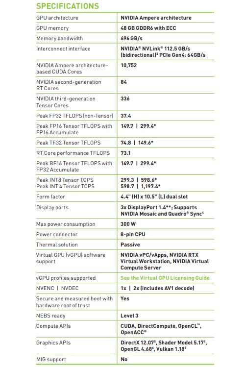
The Ampere-generation GPU itself is a GA102-895 with a 1305MHz base and a 1740MHz boost clock and 10,752 CUDA cores. The 48GB of memory is GDDR6 at 7250MHz and with a 384-bit wide bus width for a total of 696GB/s of peak memory bandwidth. We also get ECC memory in this class of GPU. Here are the full specs:
Next, we are going to take a quick look at performance before we move on to power consumption and topology.


 and show some of its interesting features)
This GPU is rated 0.5 TFlops double precision with single precision an astonishing 64 times faster than double.
For reference a lowly Radeon VII yields 3.3 TFlops of double precision which is about 6 times faster than the A40.
In my opinion the level of market segmentation that Nvidia is practicing with their GPUs right now can’t be good for anyone but Nvidia.
Since the main advantage GPGPU computing has over special-purpose neural network hardware is that GP stands for general purpose, it would be useful to test a comprehensive selection of general application domains in the GPU reviews. Such tests are especially important for GPUs with intentionally lopsided capabilities that target very specific market segments.
What your pair of bar charts are supposed to mean?
Are you comparing the A40 cards on hand to past A40s you’ve tested? Are you comparing the same cards running in different servers (ie the charts are actually server comparisons?)
Anyway, A40 (A10, A6000) have negligible FP64 ability but superior FP32. A100 is an FP64 monster with relatively modest FP32.
Ironically, you seem to think you are complaining about too much market segmentation but in fact you are complaining about not enough. Additionally, more segmentation of the type you are looking for would result in more expensive parts, or simply the market not being served at all. Most GPU domains do not require FP64 operations. The A40 is based on the GA102 GPU which is the top-of-the-line graphics/gaming oriented GPU from NVIDIA. By including full FP64 on it, it would lose performance in its core markets: gaming and professional graphics. If you want FP64 on a data center NVIDIA GPU less powerful than an A100 then you have to go for the A30 or for an older generation Gx100 GPU. If you want both ray tracing and full FP64 on the same GPU then you must either go to another manufacturer or convince NVIDIA that the size of your market is large enough to either 1) warrant NVIDIA spending hundreds of millions of dollars to make a special GPU for the market or 2) warrant NVIDIA spending money to add ray tracing to all data center GPUs and reducing the CUDA performance somewhat in the process due to the loss of die area and sacrifices that must be made to optimize for a greater set of constraints.
@Matt I don’t think OP was thinking that FP64 uses dedicated silicon, and I don’t think so either. In the earlier days of Quadro (think Kepler) the Titan used the same chip, but had FP64 cut by 2/3.
@steffen It does use dedicated silicon as NVIDIA architects it now. If I remember, in Kepler FP64 also used dedicated silicon. They cut the FP64 rate in firmware for differentiation purposes, as did AMD. In the Tesla (architecture, not product line) generation, and maybe in Fermi, NVIDIA had FP32 units built into their FP64 units and so didn’t use as much extra die area for the FP64. However, I believe that’s less energy efficient and that’s why they changed it. Or perhaps they changed it for some other reason, such as easier optimization or ability to reach higher clock speeds. Regardless, AMD followed suit. Also, the fact that AMD produced the Radeon VII (in extremely low quantities) has no bearing on the fundamental physics. AMD was looking for markets for chips. The card sucked for most use cases and, as noted, was produced in very low quantities. If anything it can be used as evidence that use case differentiation in the GPU space is very real. There’s so much “conspiracy theory” online when it comes to Nvidia. It’s tiresome.
Comments are closed.