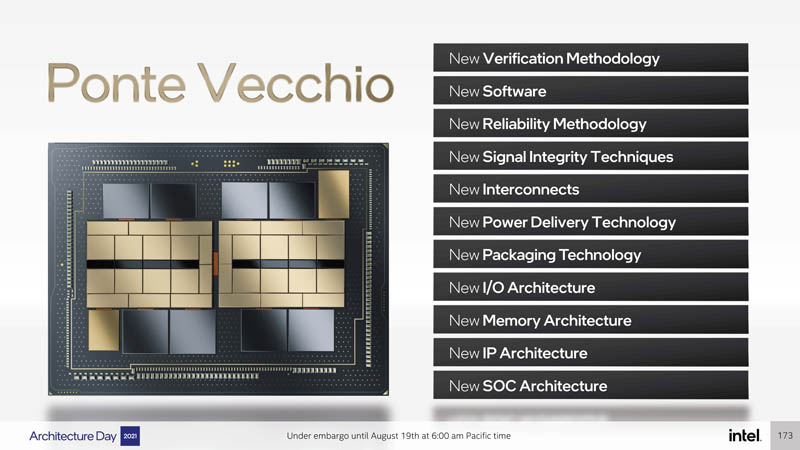
Intel Ponte Vecchio Chipbuilding
Whereas we just focused on the lower-level architecture, which in many ways was coming up with lots of bandwidth and lots of vector/ matrix compute resources. Perhaps the bigger marvel is how Ponte Vecchio went from those base units to a usable chip. Ponte Vecchio is made up of dozens of smaller tiles and chips, from different fabs and on different process nodes. Intel had to do a lot of innovation to turn this concept into something useful.
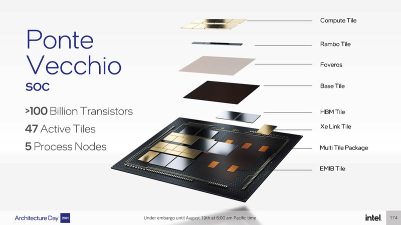
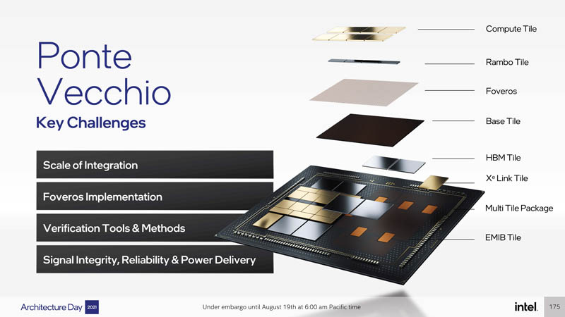
In summary, we have a chip with over 100 billion transistors, 47 active tiles (e.g. excluding structural components) and using 5 different process nodes.
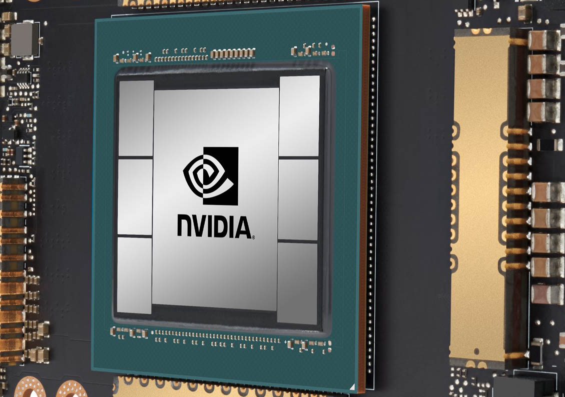
As a point of reference, the NVIDIA A100 is basically a GPU die, six HBM2(e) packages, and the connective tissue between those components. This is NVIDIA’s current state of the art for reference.
As one can imagine that created new challenges.
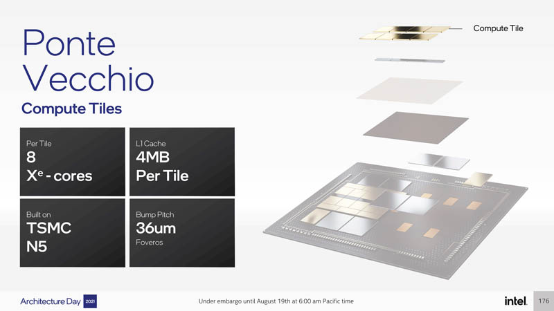
The compute tiles are made up of 8x Xe HPC cores. If you open the previous page with the architecture you can basically tie the components as we went from core to slice and so forth with the SoC components here. For example, we have 8x Xe Cores per tile. We know that we have sixteen of these cores in a slice and then as these slices become a stack we get L2 cache and there is a Rambo cache tile being shown. If you put both side-by-side they make a lot of sense.
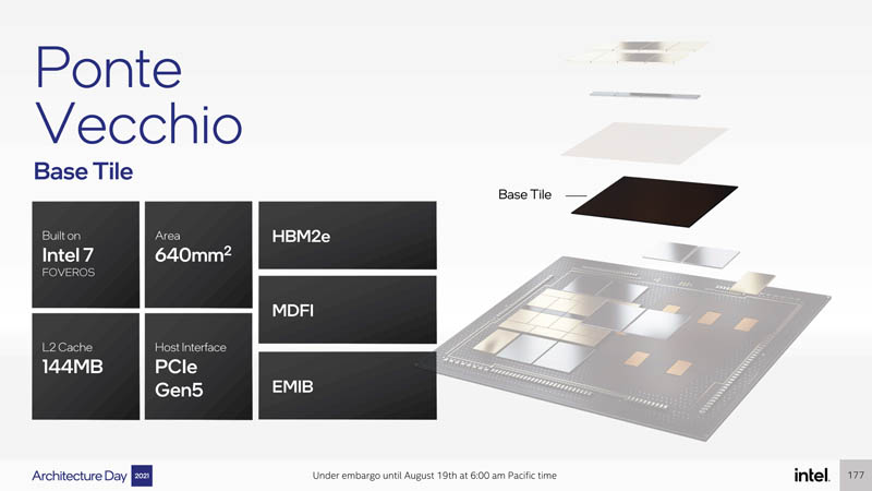
While the compute tile is based on TSMC N5, the Ponte Vecchio Base Tile is on Intel 7. We also see that we have 144MB of L2 cache and a PCIe Gen5 interface. Intel did not say that this is a CXL device, although CXL 1.1 is focused on PCIe Gen5 generation parts and the key use case as outlined in its Intel Hot Interconnects 2021 CXL Keynote is for GPUs and accelerators.
We discussed Xe link but this is based on TSMC N7. Typically we see SerDes and switch tiles on older nodes as they can be harder to scale.

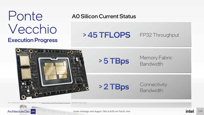
Intel says that it is getting over 45 FP32 TFLOPS per GPU using early A0 silicon. During its presentation, Intel made it seem like these figures had room to go up in production versions. Intel also has some massive interconnect and memory bandwidth.
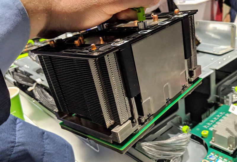
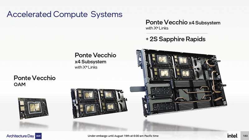
Intel is showing OAM modules and we covered how Intel Xeon Sapphire Rapids Supports HBM and Ponte Vecchio OAM Update. OAM is a next-generation form factor designed for 600W+ accelerators from multiple companies as an answer to the NVIDIA SXM4 modules. Here is an OAM cooler for example.
These fit into larger assemblies that allow GPU-to-GPU links and very interesting topologies. For example, we saw the Inspur OAM UBB as an 8x GPU design and looked at others using the Universal Base Board (UBB.)
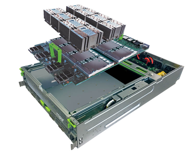
Intel will also sell four GPU assemblies in addition to the 8x GPU and 6x GPU configurations.
We will quickly note that the Ponte Vecchio system being shown with Sapphire Rapids is being liquid-cooled. We recently did our Liquid Cooling Next-Gen Servers Getting Hands-on with 3 Options piece to help get our readers ready for next-year’s transition.
Even the Aurora Exascale supercomputer blade is liquid-cooled with 6x of these GPUs and two Sapphire Rapids CPUs. There is a not-so-subtle pattern afoot.

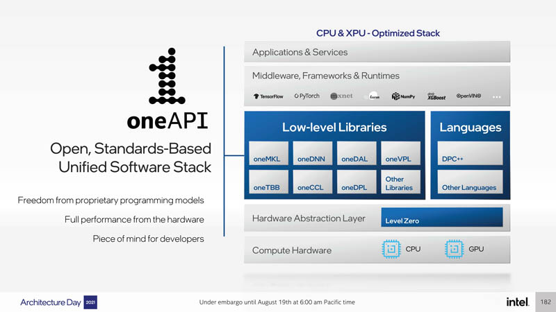
A big part of Intel’s efforts is around software and oneAPI. Intel’s goal is to have programmers build code and then run it on the right acceleration platform as seamlessly as possible. The key here is that Intel is trying to make a CUDA competitor for the industry that works across more than just its Ponte Vecchio GPUs.
Overall, this is a hugely ambitious project and Intel is integrating significantly more tiles from more process nodes and in a more complex fashion. The goal is that all of this chipbuilding work yields something that is a step function better instead of a 10-20% improvement.
Final Words
The entire industry should be nothing short of excited for Ponte Vecchio. Just the fact that Intel is producing this complex piece of engineering and getting awesome performance from it means that as a scientist and/ or customer, you should be excited. Intel is betting that its oneAPI software stack will help onboard developers and code from CUDA to Intel’s GPU compute. Still, having this massive of a GPU out there means that both NVIDIA and AMD are going to need the next generation of data center GPUs to have a step function of performance improvement. We know that AMD has something special with its next-generation parts that were the driving force behind AMD winning two of the first three Department of Energy Exascale systems. For NVIDIA, we may actually have a competition coming to the data center space.
Again, we are going to say that the level of integration of this chip is well beyond other products being sold on the market today. The fact that these are becoming commercial products means that the entire industry will be forced to change the way it designs chips. Like a spaceship that hurdles mankind into the heavens to new frontiers of exploration, Ponte Vecchio will thrust humanity into a new era of compute design.


Quanta costa… I guess not cheap GPUs these Ponte Vecchio
“The Xe Link is the high-speed coherent unified fabric …”
Previous presentations on Ponte Vecchio mentioned CXL, and I presumed the Sapphire Rapids chips would be responsible for coherency. I didn’t hear CXL mentioned for Ponte Vecchio today, nor for any of the other chips except Sapphire Rapids.
It seems there are late on cache coherency compared to AMD which handle it between EPYC and Instinct MI200
“Like a spaceship that hurdles mankind”…
Surely you mean hurls?
Can it run Crysis, tho?
Intel bought up most of tscm 3 nm production lul who cares what amd does
Comments are closed.