
At OCP Summit 2019, we showed the 10nm Intel NNP I-1000 M.2 and why it is likely Facebook’s AI inferencing solution. We even showed the “Glacier Point V2” in that article that showed a very dense M.2 solution. Five months later at Hot Chips 31, Intel is providing more details on the Intel NNP-I 1000. One will not that at OCP Summit this was the “NNP I-1000” but the dash has migrated and it is now the “NNP-I 1000”.
Intel NNP-I 1000 Spring Hill Overview
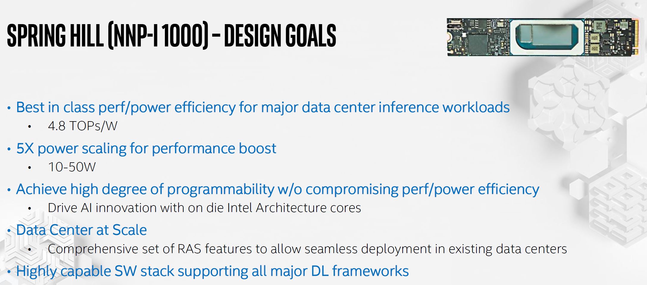
At Hot Chips 31, the company outlined the product codenamed “Spring Hill” which is now called the Intel NNP-I 1000. One of the big design goals was to get around 5 TOPs/W. Intel says that it settled on 4.8 TOPs/W. It also chose not to make the NNP-I 1000 a super low-power (e.g. phone/ IoT device) range of total power consumption. That is how it decided on the 10-50W range.
Key to the NNP-I 1000 are the ICE units (more on those soon.) There is a 24MB LLC that is on the coherent fabric. The two SNC IA Core are Sunny Cove x86 cores are on the same fabric and share the same cache. These Sunny Cove cores also increase the flexibility of the cores. Intel also built-in some orchestration activities in hardware to increase performance.
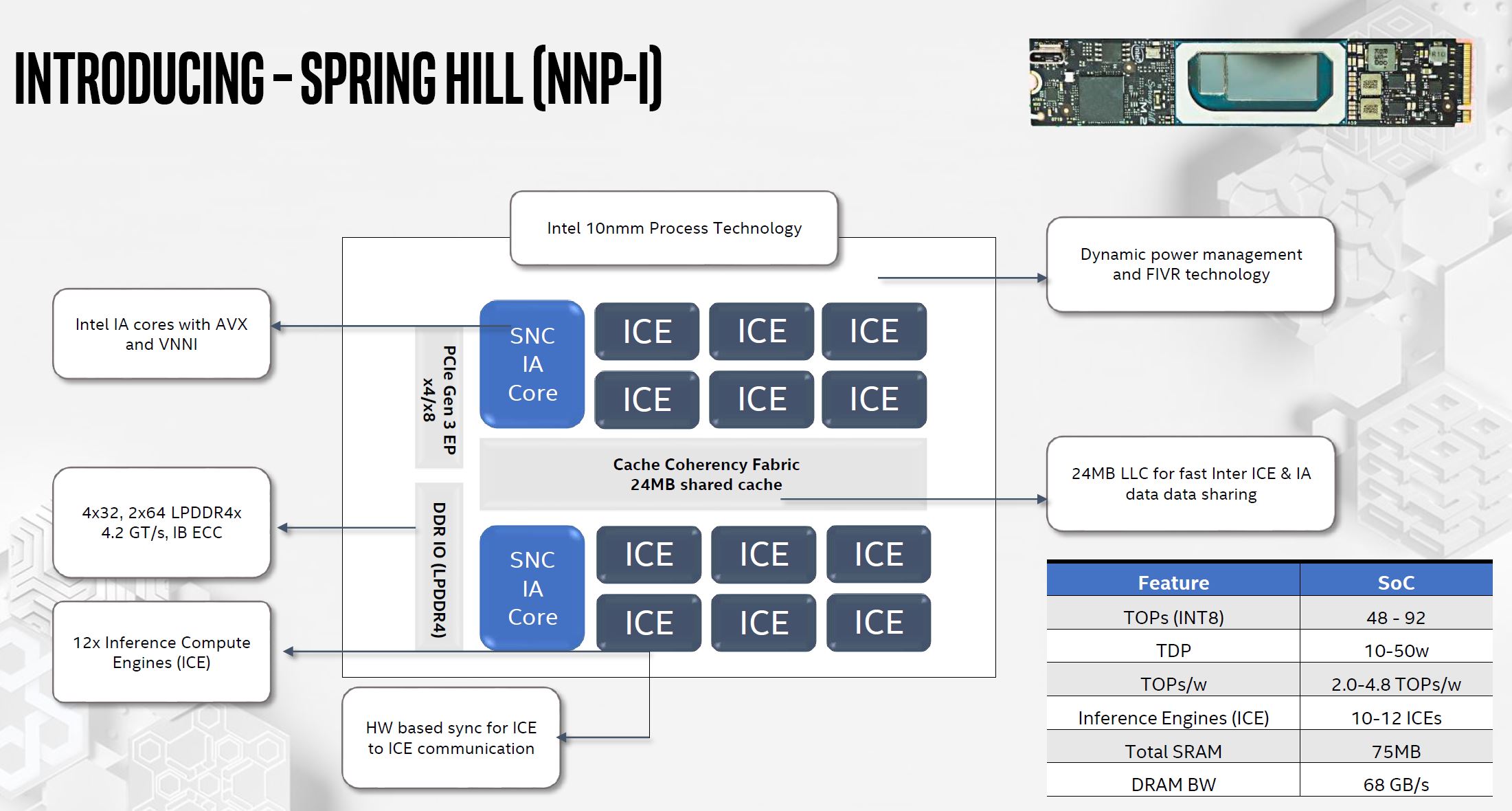
For power management, Spring Hill can shift power budget. One will notice FIVR appears in this design as well. It is a standard PCIe Gen3 device and Intel says this is enough bandwidth. There are 128 DDR lanes (e.g. LPDDR4x in this case.) There is a total of 75MB of SRAM onboard which absorbs most of the memory needs. This is similar to how others are architecting high SRAM to increase effective memory bandwidth.
An Intel Inference Compute Engine (ICE) is the key deep learning accelerator. ICE units have 4MB of SRAM for buffering data movement. Intel also has various math types it supports leading to flexibility. FP32 and FP64 are not present based on Intel’s Hot Chips talk and slide.
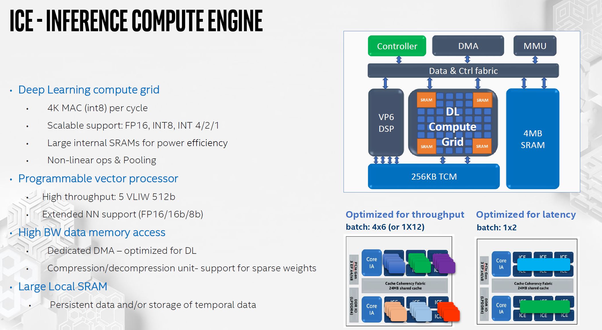
Zooming into the DL Compute Grid. Intel says this has “four dimensions of parallelism.” This structure minimizes data movement. Every element that is read, it is used multiple times in the structure. The I/O buffers maximize the amount of time that the computation sits in the DL Compute Grid.
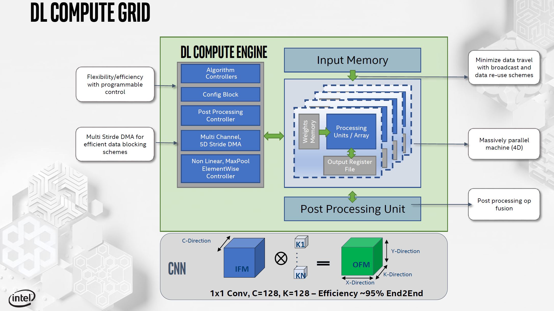
Post-processing allows Intel to do things like fuse layers to avoid going back to memory. This is controlled by the Post-processing Controller. A key to this is that Intel expects the compiler will help optimize for its ICE and DL Compute Grid.
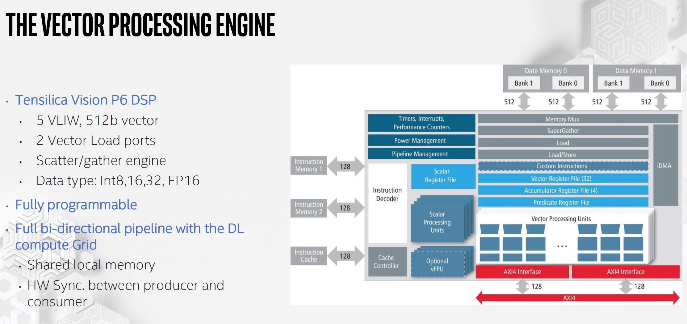
This is a customized DSP block called the Vector Processing Engine. It is meant to work alongside the DL Compute Grid with features like hardware sync and shared local memory.
There are four levels of memory that the Intel NNP-I 1000 supports with increasing bandwidth. LPDDR4 is the first level. Last level cache is about 10x that. Internal SRAM provides about 100x LPDDR4 bandwidth. Within compute engines, memory is even faster.

To orchestrate this, the compiler needs to do things like place work on the vector engine and the ICE.
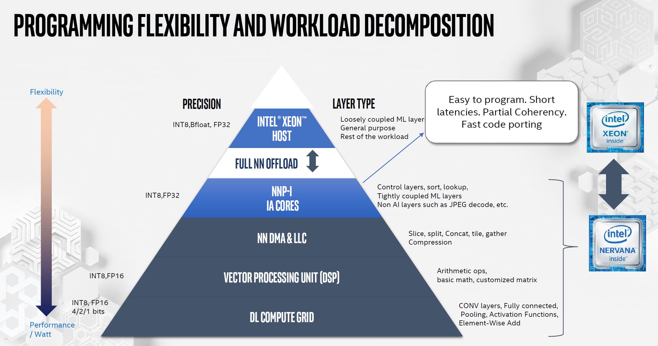
The talk is going fast, but a key feature here is that Intel needs tight software and hardware integration to place work efficiently and keep the engines fed.
Performance and Key Challenge Intel is Facing
Here is Intel’s performance slide which is perhaps the most colorful 3D bar chart ever made.
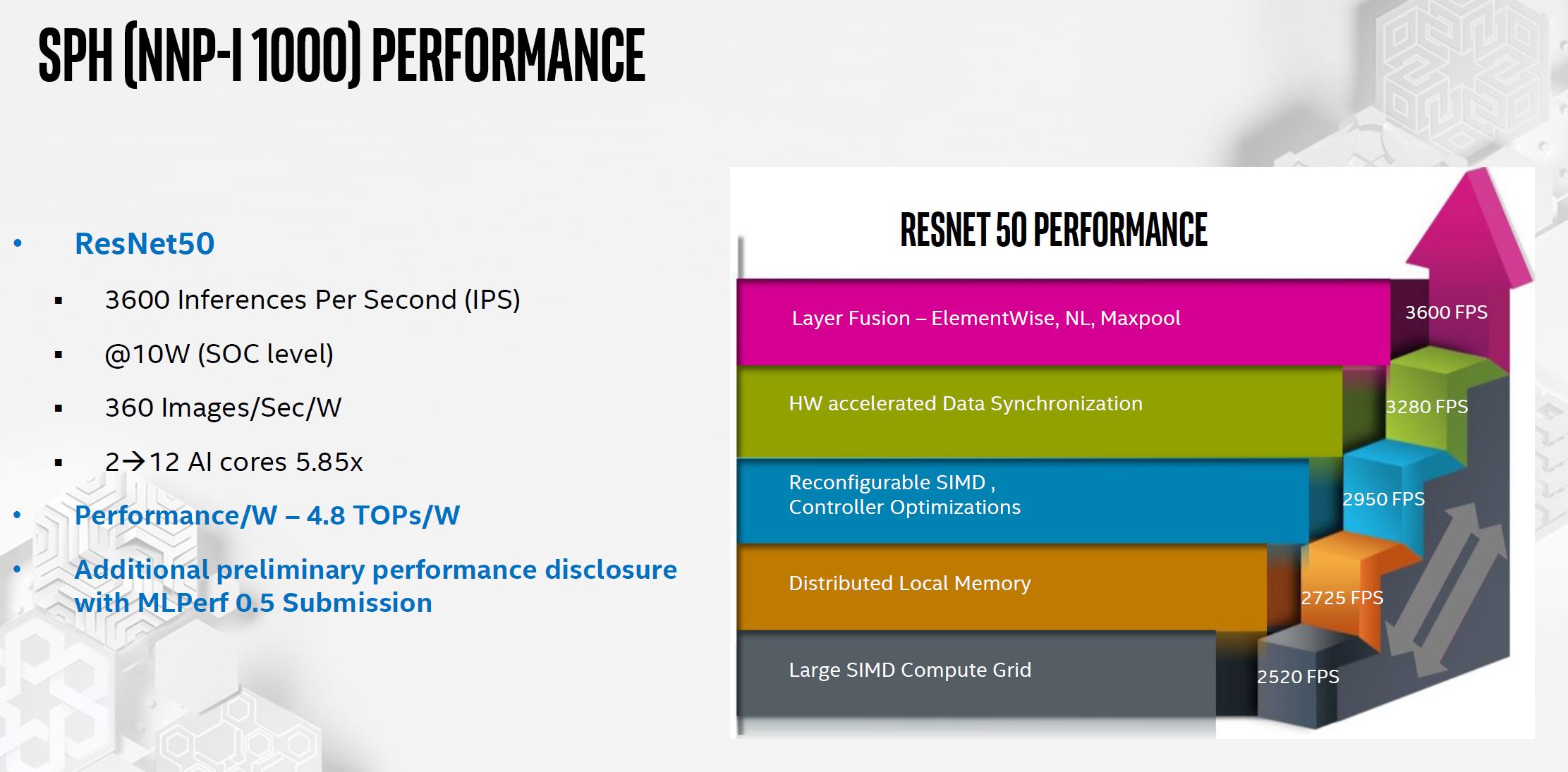
Intel says it can get close to linear scaling beyond this 2-core configuration. Intel has tested scaling up to 12 cores and gets 5.85x performance uplift. As a result, it thinks that the design is scalable.
You will notice that the 10W is at the dual-core SoC level, not at the M.2 assembly level. That presents the big challenge that Intel is facing with the NNP-I 1000: cooling.
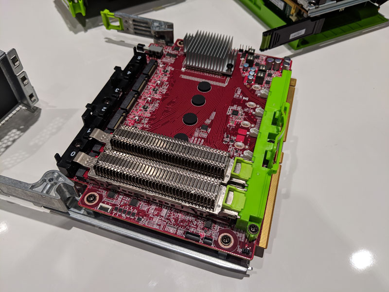
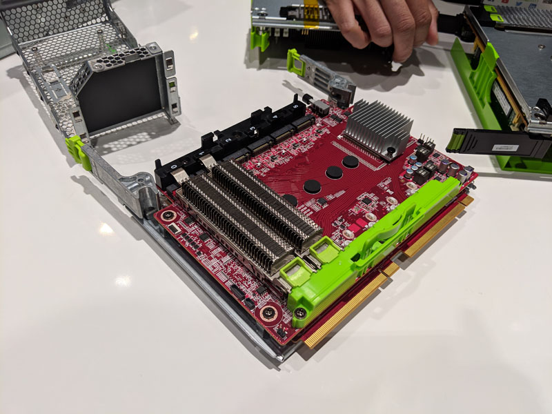
It turns out that the Facebook OCP Yosemite V2 chassis were not necessarily designed for this many higher-power M.2 cards. The Intel NNP-I 1000 M.2, and more importantly, many NNP-I 1000 cards can use a lot of power. With the M.2 spec and spacing in the chassis, cooling has been a challenge. Although this was not in the talk, we have heard a lot of industry chatter that the Intel and Facebook teams have had to work hard to ensure these can be cooled in a chassis that was designed to cool the Twin Lakes Intel Xeon D-2100 Platform, along with M.2 SSD cartridges. The minimal heatsink space and airflow in the chassis presented a significant challenge.
Final Words
Intel is in the process of building large Intel Nervana NNP training systems. Outside of that portfolio, AI inferencing is being integrated everywhere. With an M.2 form factor, the hope is that the Intel NNP-I 1000 Spring Hill platform can provide low power accelerators beyond what is available in the company’s CPU cores.


