
Graphcore is presenting its new IPU at Hot Chips 33. We have covered the Mk2 in our Graphcore GC200 IPU launch. We have also covered how confusingly similar Intel’s new use of IPU in an adjacent space is to what Graphcore has been using for years. Finally, we have covered how Graphcore celebrated a stunning loss at MLPerf Training v1.0. Still, we wanted to cover the Hot Chips 33 talk on their progress. As with others, this is being done live so please excuse typos.
Graphcore Colossus Mk2 IPU at Hot Chips 33
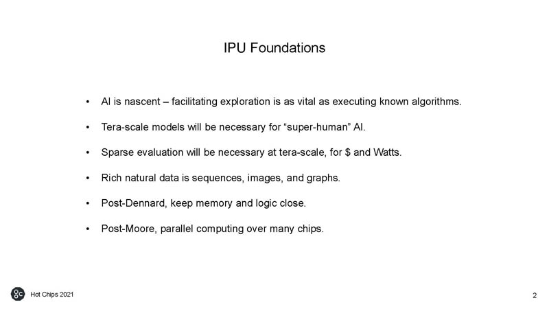
Graphcore has a ton of slides, at around 1 slide per minute for its talk. As a result, we are going to let you read a few slides to keep pace for the rest of the day. One of those is the foundations of Graphcore’s IPU (as opposed to Intel’s IPUs that are really DPUs.)
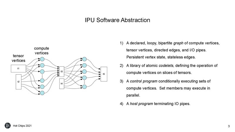
The next two we will let you read with the context that Graphcore has been working on developing a software stack seemingly with more effort than its hardware stack so the software side is important.
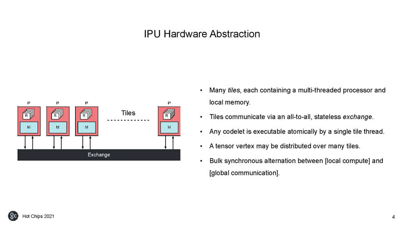
As with many AI chips, Graphcore has many processors with many threads and a solution to feed those processors via high-speed memory.
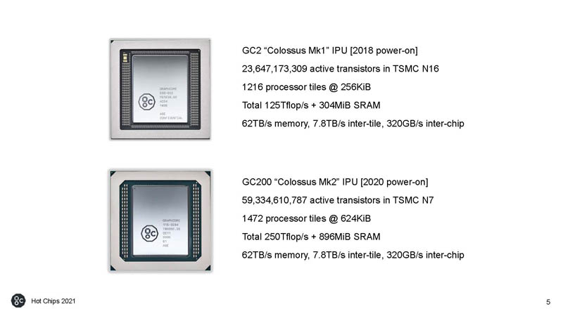
For some reference, the number of processor tiles did not increase dramatically, but the shrink from TSMC16 to TSMC7 seems to have had a huge impact on SRAM size while also doubling compute.
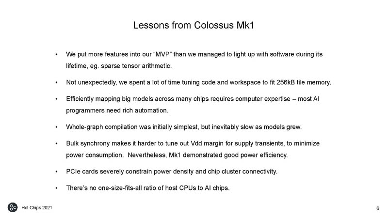
Here are the key lessons learned. The PCIe power density constraint is worth highlighting since at STH we have been doing a lot of work reviewing SXM4 A100 systems like the Inspur NF5488A5 and Dell EMC PowerEdge XE8545 recently and have been covering OAM solutions like the Intel Ponte Vecchio Spaceship GPU. We have certainly seen the impact of PCIe constraints first-hand.
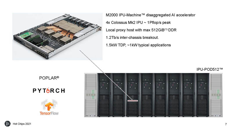
The M2000 IPU-Machine takes four Colossus Mk2 IPUs and puts them into a chassis with a controller and 512GB of local memory. There is also an interconnect to other nodes.
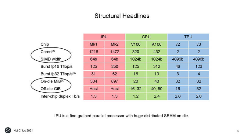
Here is the structural highlight between the Graphcore, NVIDIA, and Google TPU options. Most use different units so this is always hard to compare.
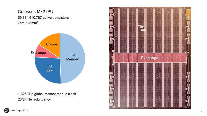
Here is a look at the IPU. This is the Colossus Mk2 IPU with over 59B transistors in TSMC 7nm. The 23/24 redundancy means that there is a spare tile for every 23 active tiles.
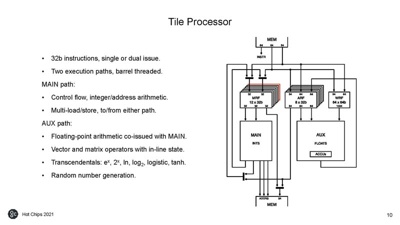
This is the basics behind the Graphcore IPU Tile Processor.
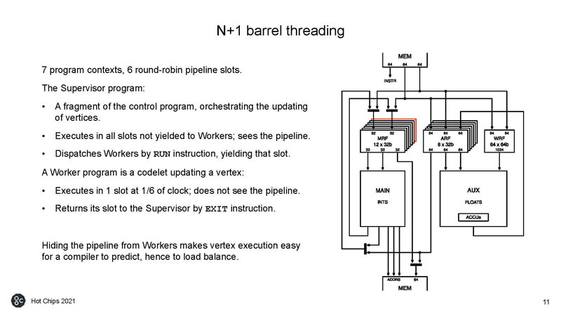
Here is a look at the threading.
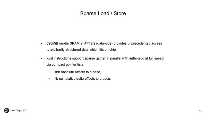
Graphcore can maximize memory utilization with its sparse load/ store.
Graphcore above focused on its FP32 performance compared to the NVIDIA A100 and other chips. Here is how that works.
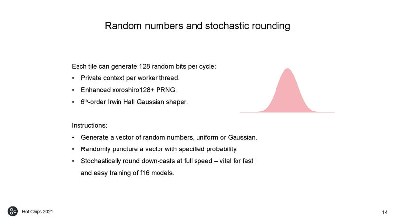
The chips can also generate random numbers.
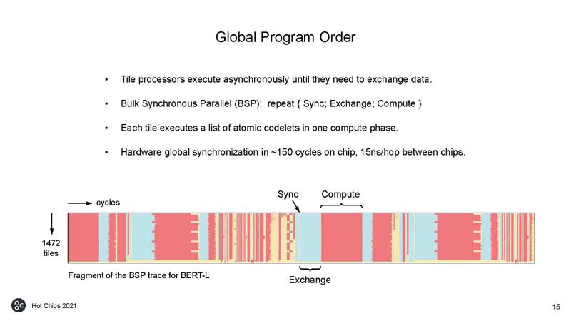
The tiles execute instructions asynchronously and then data is synchronized when the exchange between chips must happen.
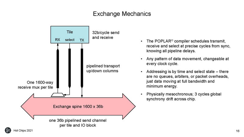
Here is how that exchange occurs.
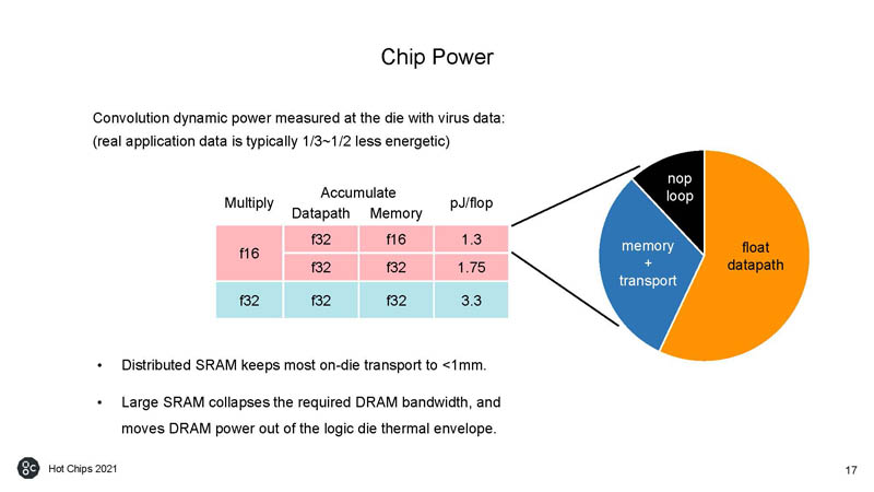
On the chip power side, here is the power consumption of the chip. Specifically interesting is how much is used by the memory and transport functions.
Here is the TFLOP per Watt. Graphcore shows it is pushing more than NVIDIA and Google.

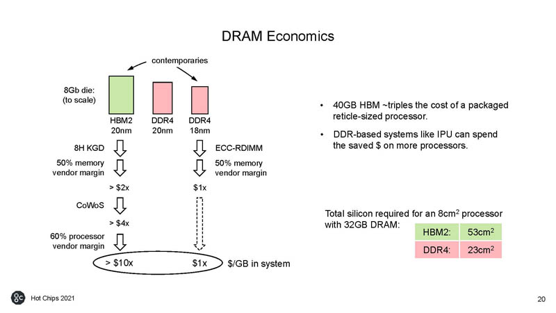
One of the big questions is why not use HBM. Graphcore says that it is expensive and capacity-limited. HBM2e is not the main reason that the NVIDIA A100 80GB is well over $10,000 each.
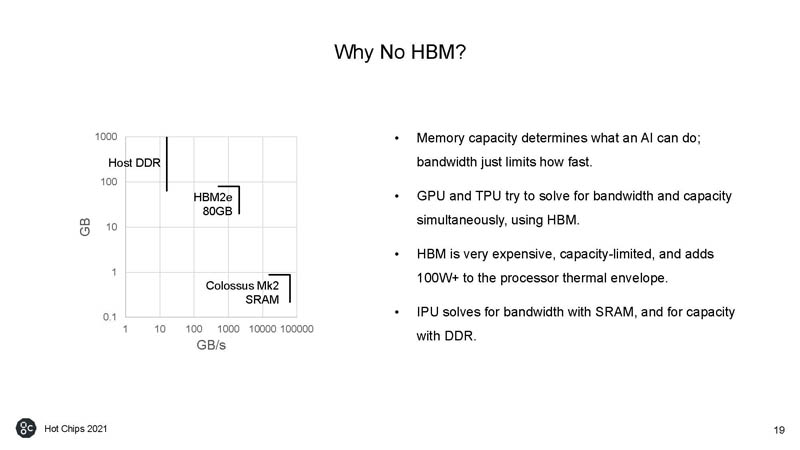
Effectively Graphcore can make smaller less expensive chips if they use traditional DDR4 memory instead of HBM2.
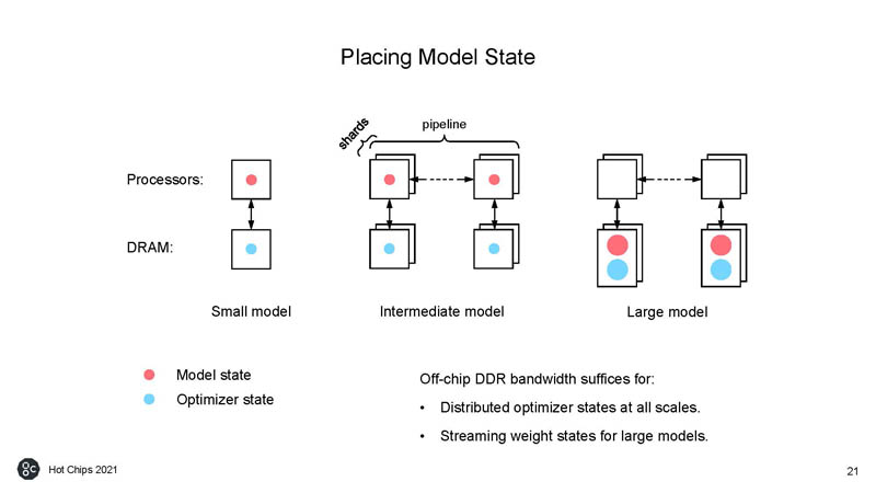
Graphcore needs to work around having a model of big SRAM and slower DDR memory instead of the more expensive HBM, so it needs to manage model state placement.
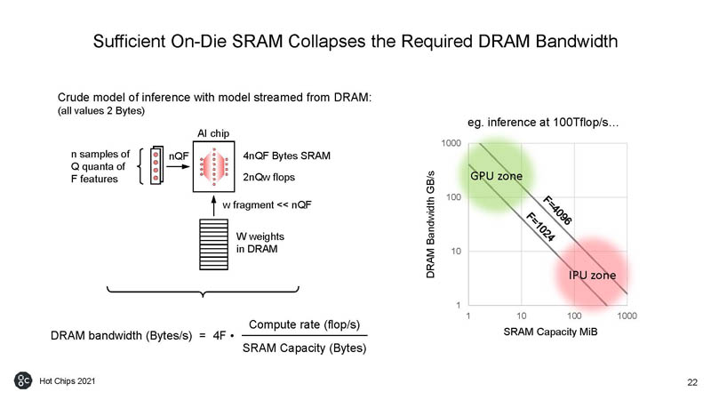
Using these techniques, Graphcore is able to have enough SRAM on die that it can minimize the performance penalty of going to off-die DRAM.
Of course, Graphcore is pushing its hardware-software work.
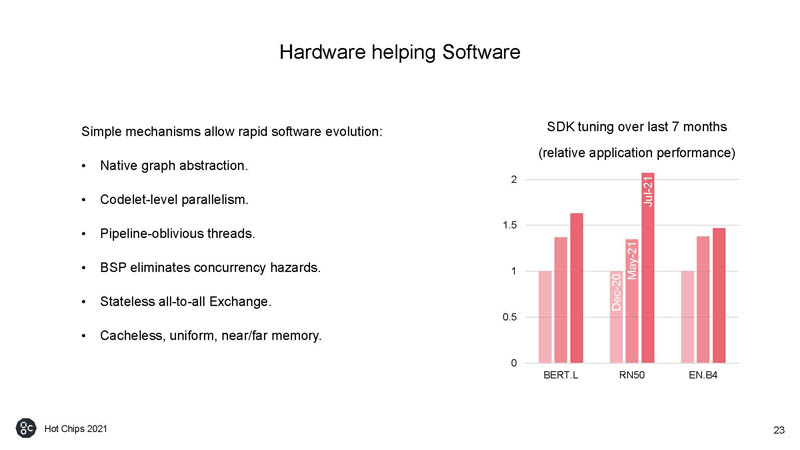
Graphcore is showing its performance gains from software. This is important since software gains can often be as big, if not bigger, than generational hardware gains.
Final Words
Overall, Graphcore has a ton of investment money. It had a poor MLPerf Training v1.0 showing with its hardware, unable to show it is clearly better than the industry standard NVIDIA A100. In this industry, one needs to be doing much better than NVIDIA to get ahead.
Also interesting, if you believe in Graphcore’s thesis of needing a lot of on-chip SRAM instead of HBM2(e) and scaling to many IPUs, then the next talk by Cerebras shows what is probably the (significantly) higher-end version of going down that path with its Wafer-Scale Engine 2.


 presentation by the company)
Interesting (or weird):
The first transistor computer had 92 transistors.
Colossus Mk2 transistors / World population =
59,334,610,787 / 7,902,068,494 = 7.50874418
92 / 7.508 = 12.25
A dozen CPUs have enough transistors to build everyone a computer.
That’s the result of 68 years of progress.
Comments are closed.