
For those that follow STH, I have been working on a concentrated line of DPU coverage for several months. If you are not yet familiar with the term, see our What is a DPU or data processing unit? piece. One of the promising areas for DPUs to disrupt the status quo is in storage. Today, Fungible embarks on that journey with their DPU-based storage cluster. Since this is STH, we are going to cover the news, but we got to see the solution hands-on last week and have some video to share as well. Let us take a look at the Fungible DPU-based storage cluster and the FS1600 DPU-storage node to see why this is something to get excited about.
Video Hands-on Look
This article has something a bit different. Normally, our web and video content match fairly closely. For this piece, we have a bit more on the video side:
In this video, we talk about the technology, but then also have an interview with Fungible’s CEO Pradeep Sindhu (formerly co-founder and CTO at Juniper Networks), as well as a product overview, UI look, and performance demonstration from Benny Siman-Tov Fungible’s VP of products. This is one of the rare occasions on STH where the video will have some content the web version does not have. As always, we suggest opening the video on YouTube and listening along.
Fungible DPU and TrueFabric Base
We are not going to go into too much detail here. One of Fungible’s key differentiators is the Fungible DPU. These DPUs utilize data clusters with MIPS cores, high-speed memory interfaces, accelerators, a PCIe root complex, and high-end networking to effectively move data faster and more efficiently than with traditional general-purpose CPUs such as Intel Xeon or AMD EPYC.
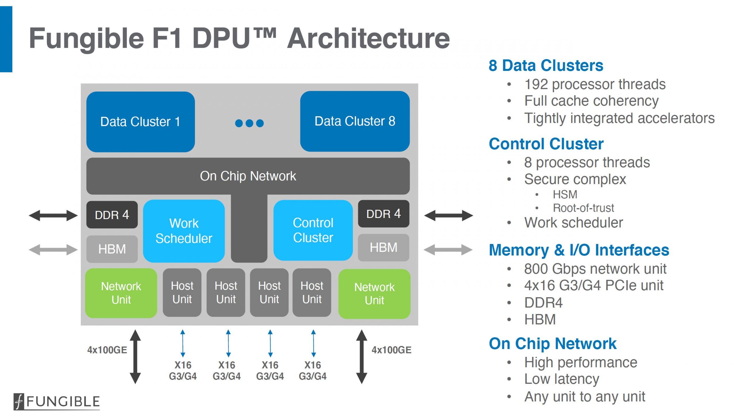
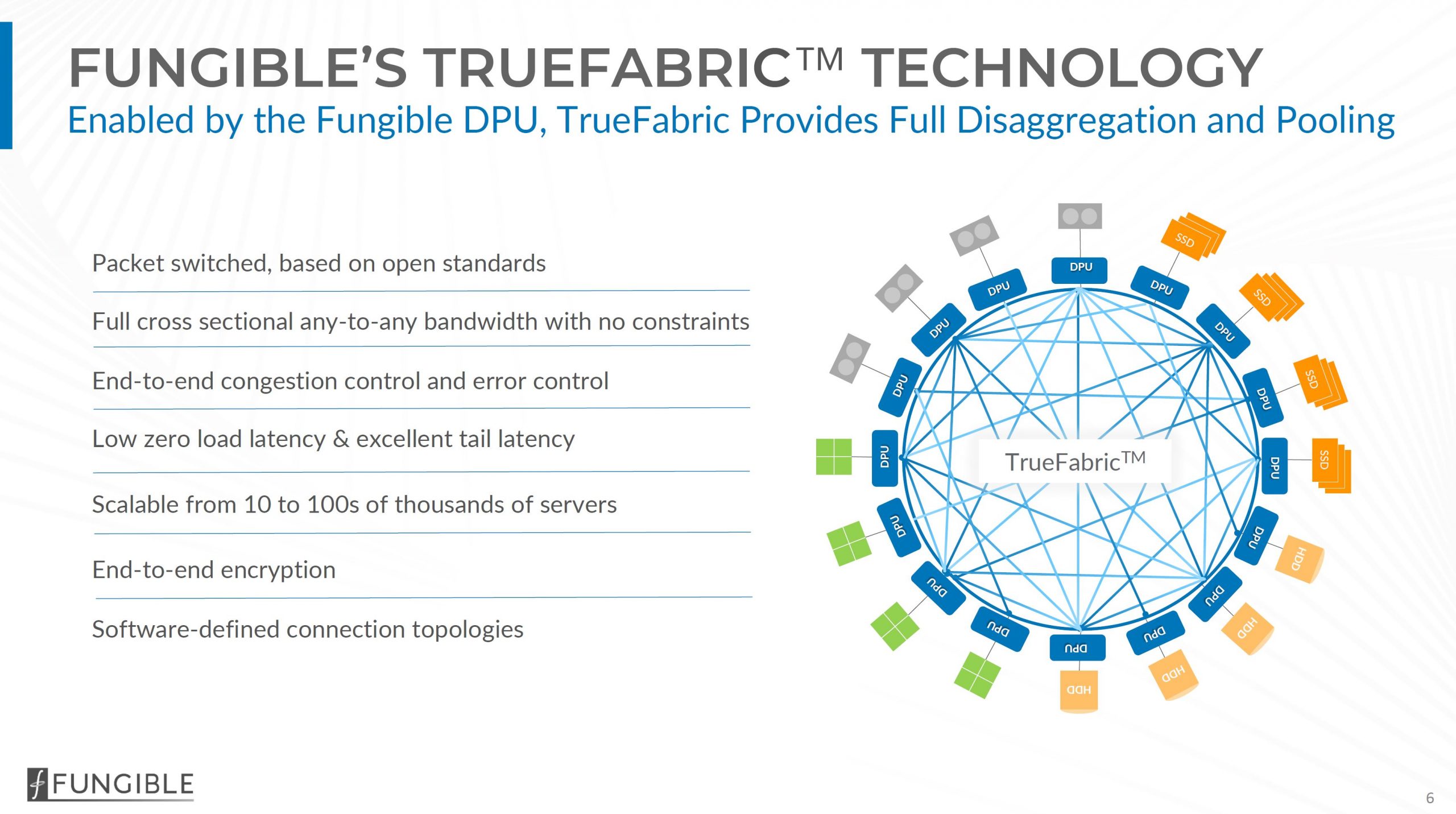
Since the folks at Fungible have a lot of networking background, not only are they focused on the endpoint processors, but they also have a data fabric called TrueFabric that is designed to handle the scaling and QoS aspects of scaling applications such as storage across DPUs.
With those base building blocks, today Fungible has its new storage cluster and DPU-based storage nodes to deliver a high-performance storage solution.
Fungible DPU-based Storage Cluster
In 2020, a single node or simple HA pair storage cluster seems less exciting. Today, efforts are focused on scale-out storage and that is where the Fungible Storage Cluster solution is designed to play. Powered by the Fungible DPU and TrueFabric, the company is solving for traditional challenges using a non-traditional architecture.
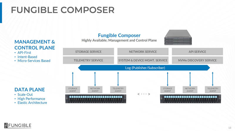
The basics of the Fungible storage cluster come down to three main components. First, there is a control plane run by the Fungible Composer nodes. Scaling out data storage involves adding more Fungible FS1600 DPU nodes which we are going to discuss later in this article and show a few hands-on photos. The third component is that the solution uses NVMeoF to connect to client servers making it relatively easy to integrate.
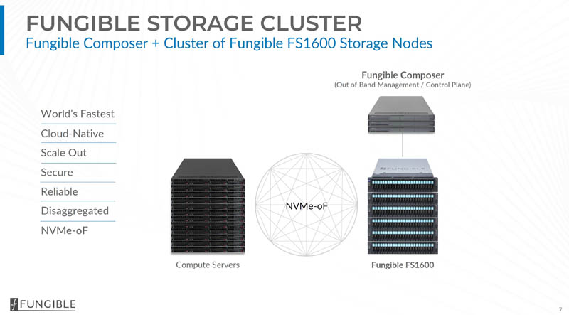
The Fungible composer runs all of the management and control planes for the solution. This is important because this abstraction of the data and management/control planes allows the solution to scale out more efficiently. While the Fungible Composer nodes we are told are more of standard servers since these are tasks where traditional models work well, the FS1600 data plane nodes are the ones with two DPUs each.
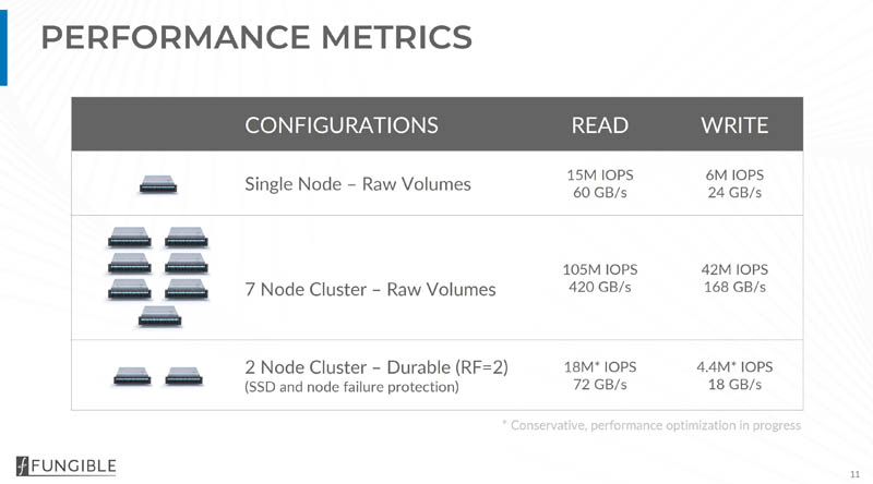
In terms of performance, here is what Fungible is claiming at a high-level:
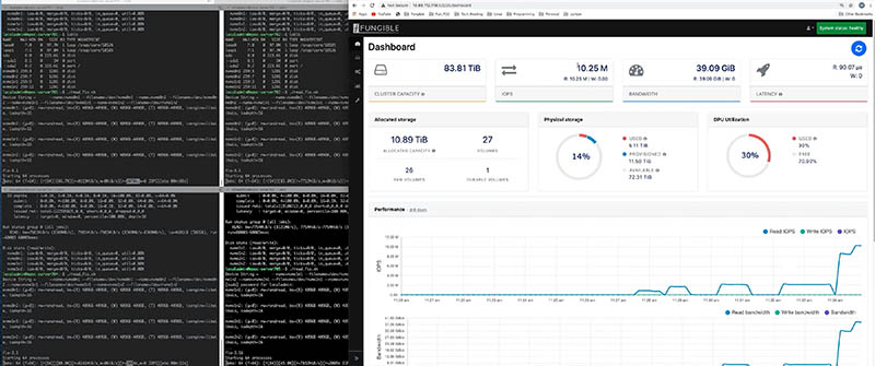
We got some hands-on time with the solution. Here is a view of a FS1600 hitting over 10M IOPS and over 39GB/s using only five server nodes as clients. One can get to higher performance using more servers making requests on the system.
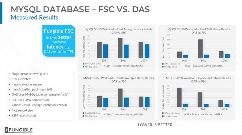
Fungible has a number of performance claims. One of the more interesting is faster database performance and lower latency than traditional direct-attached storage. Here is the MySQL slide but Fungible has Cassandra numbers it is publishing as well.
One of the key partnerships Fungible is disclosing is with IBM Spectrum Scale. With a 6-node Fungible cluster, one can get to 30M GPFSperf IOPS.
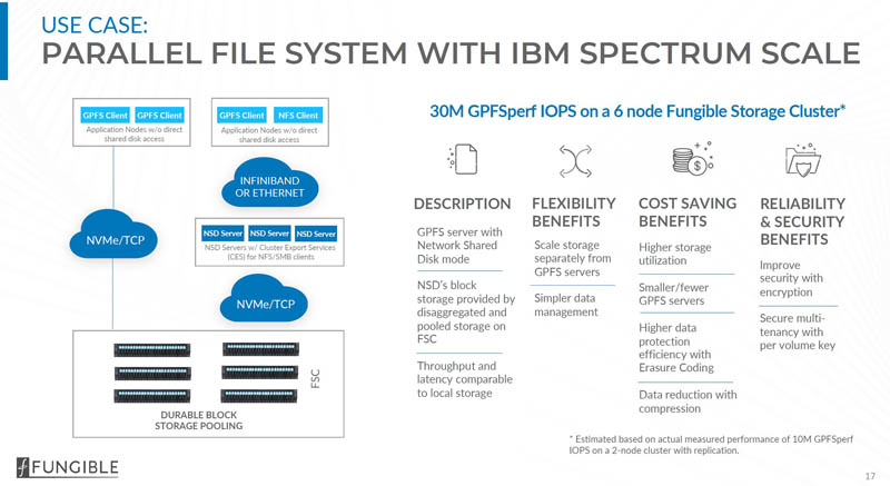
Having partnerships with companies such as IBM are important for solutions like what Fungible has here. In a stratification of storage startups, these deals with large companies help sales and marketing efforts which in turn give even well-funded startups like Fungible a path to sales. On a relative scale, having good database performance is good to show the viability of the solution, but having large sales and distribution partnerships with existing channels such as IBM are harder to get and more important.
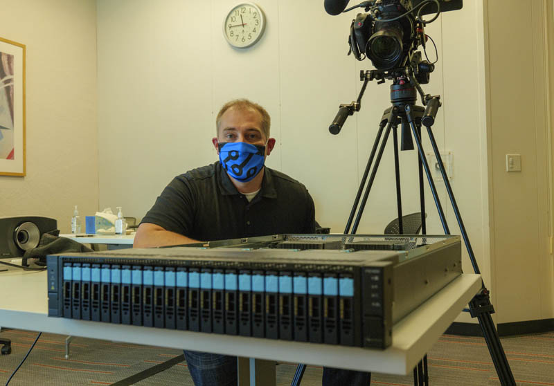
While the cluster is cool, we wanted to show off the actual DPU-based nodes themselves. As a result, we headed over to the Fungible HQ to see the Fungible FS1600 hands-on. That is also where we got the UI and fio performance demonstration screenshot above.
Fungible FS1600 Hands-on with a DPU Node
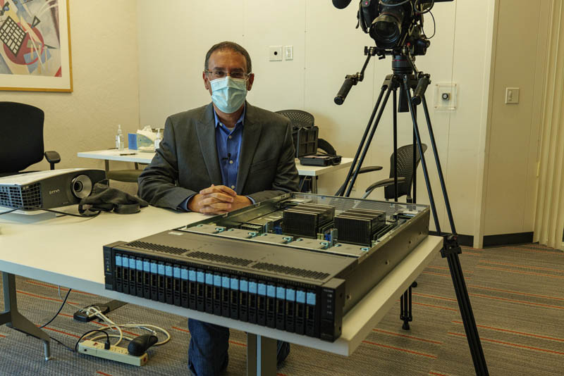
In a former MIPS Silicon Valley building, we found the Fungible headquarters. During our time there, we were able to see the Fungible FS1600 DPU-based scale-out storage node hands-on. We also have more on this and an interview with the company’s founder in the video linked above.
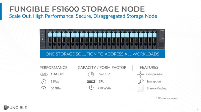
A Fungible FS1600 storage node is capable of 15M IOPS and up to 60GB/s of performance. Please note, that is in Gigabytes not Gigabits per second.
The FS1600, at some level, looks like a standard 24-bay 2.5″ NVMe enclosure we review regularly at STH. Normally, we get excited over developments such as when Dell and AMD Showcase Future of Servers 160 PCIe Lane Design in a traditional server. Here, Fungible is doing something completely different than one may expect coming from a traditional server background.
The system itself has two Fungible DPUs on a single PCB. This is not a dual-socket system in the traditional sense. Instead, each DPU works independently with its own memory, NVDIMM-N, 6x 100GbE links, and 12x of the front panel NVMe SSDs. There are a few shared features such as the ASPEED AST2500 baseboard management controller (or BMC) along with an Intel-Altera FPGA for features such as status LED blinking and enclosure management. The other major shared features are the power and cooling since there are two power supplies to provide redundancy and five chassis fans for cooling.
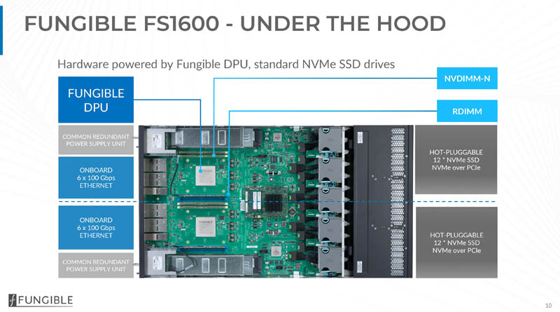
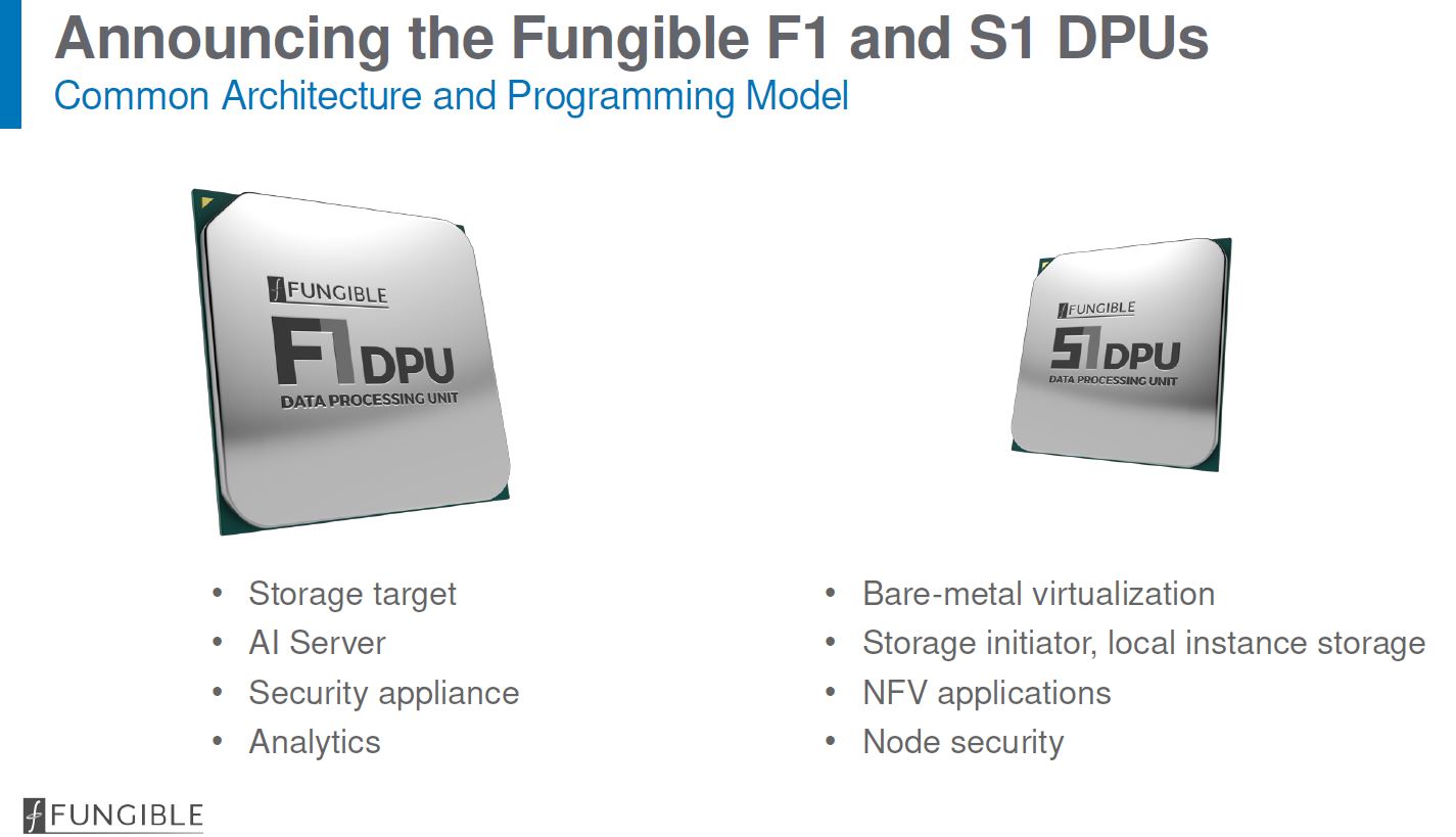
The two DPUs effectively run as independent nodes for purposes of running the scale-out data plane. Each DPU is specifically designed for scale-out storage and to accelerate storage and retrieval of data on the NVMe SSDs. If you want to learn more about the Fungible F1 DPU features and architecture, see our Fungible F1 DPU article.
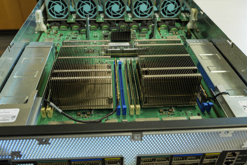
Here is another look at the system there is a COM card with a traditional embedded node in the center of the system. We are using a revision 2 chassis for this hands-on so this card that was mostly for bring-up and development is present. In future generations, we were told these will be removed.
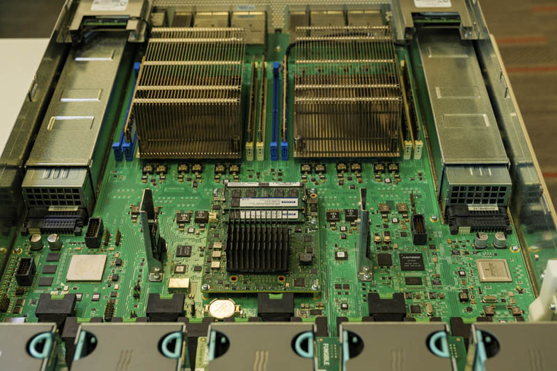
A few quick notes here. First, the DPU heatsinks are large. After seeing this unit I looked at an AMD EPYC heatsink and fan say they are the same order of magnitude in size. These are not simple low-end PCIe NIC heatsinks. Instead, the correct way to view the Fungible DPU is that it is a combination of a specialized processor, accelerators, and connectivity. One will notice that there are no standard PCIe slots in this system which means there are no PCIe NICs or storage controllers. The three main serviceable types of components are the
- 24x NVMe SSDs
- 2x Boot storage modules
- 2x Power supplies
- DDR4 RDIMMs
- NVDIMM-N’s with their energy storage modules (Agigatech in this system)
The level of integration with the DPU versus a traditional Arm or Intel/ AMD server is much higher.
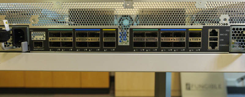
On the official Fungible documentation, we see there are 6x 100GbE ports on the back of the system per DPU. In this revision, there are actually ten 100Gbps ports per DPU for 20 total. This view almost looks like something we would expect to see from an early 100Gbps switch instead of on a storage appliance. That is perhaps the point though. Traditional servers struggle with the memory bandwidth, and certainly the inter-socket bandwidth constraints of high-end NVMe storage solutions and high-end networking. We have features such as RDMA/ RoCE to help with this, but there are fundamental bandwidth limitations we run into. The DPU is designed for this application so it can design for these bandwidth challenges. In addition, accelerators for networking as well as encryption/ compression can be added with line-rate performance targets.
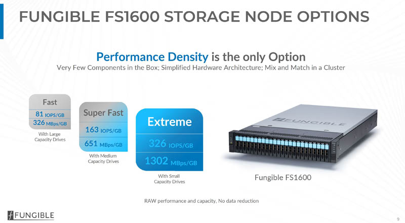
Fungible offers a number of different options focused on storage density. One can get higher capacity drives with less performance per GB or smaller capacity drives in the system with higher performance per GB.
Again, if you want to hear it from Fungible, in the video linked above we have Benny Siman-Tov, the VP of product for Fungible going over the solution.
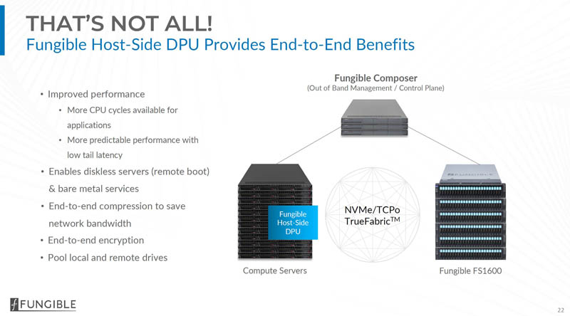
Next-Step Client TrueFabric with Host-Side DPUs
What we did not get to cover is the host-side DPU. If you remember the TrueFabric discussion above, Fungible’s vision extends beyond the storage solution running on standard 100GbE networks. Fungible also envisions tightly controlling features such as quality of service using TrueFabric.
We somewhat knew this was coming since at the company’s Hot Chips 32 presentation we saw that there would be the Fungible S1 DPU.
Having a DPU on the host side also allows for features such as turning the x86 or Arm serve as a bare-metal resource that can be provisioned as an entire server. The host-side DPU can present itself to the server as a network interface and a NVMe device, and then TrueFabric and the Fungible Storage solution can orchestrate storage and parts of the provisioning process. The industry is moving toward a model with these host cards after AWS Nitro paved the way, so for cloud providers that need a similar infrastructure, Fungible will have a DPU-based solution.
Final Words
First, I wanted to thank the Fungible team for arranging this. It was great to not only see the slideware but to also see a system in-person.
A few items truly stood out from the hardware side. The DPU heatsinks were very large. It is right to think of these as in-line with modern CPUs or GPUs in terms of what they are accomplishing. Perhaps the most shocking change was seeing a system that looks like a server, and normally we would expect to see a standard server in, yet it has no PCIe expansion. That was a different experience. Designing something different is a means, but the end is delivering high-performance at scale which we saw from the performance demo.
Stay tuned for more Fungible and DPU coverage on STH. Our next goal is to see if we can look at the Fungible S1 host-side solution.


Seriously handicapping MySQL on DAS by using InnoDB zlib compression (without any accelerator) seems like a dirty trick to me.
No NICs? It seems to have 4 count 100Gb/s Ethernet interfaces. By this logic my Asus mobos have no NICs because the Ethernet controller is solderex to the board.
hoohoo they’re in the DPU
Nils,
OF course I couldn’t be ignorant of decade long efforts to turn non ACID compliant non conforming databases into purportedly robust enterprise class database management systems.
I’m not seeking adversarial postulation here at all but I think it’s time in the current generation cycle of on boarding new recruits and younger still than us cultures and yet greater distancing between the exposure to advanced computers and sophisticated matured and enterprise endogenous feature complete except for large sure request actively managed database production systems running 9 figure budgets thru the fiscal year not startup notional down rounds.
I need to say something to remark how I representative I think MYSQL is of where something like this 1600 mix will be welcomed with a surprise particular of loving arms : shops with big ETL jobs whose the first high millions IOPS box now year’s ago that was snapped up by Dell I think and the brand cancelled beyond the single astounding product. IBM 9000 moniker after acquisition possibly but surely was Dell acquihiring as EMC integrated
If I can get testable P4 codes (state machine in simplicity I recall but I must admit I’m mixing with the P declarative language of Excel and Windows USB drivers also a super format wrangler) which I can gate for gate line for line up thru the entire stack thrown every kind of torture at and it surfaces sweetly, I know people who will hang these things between Superdome VMS clusters to cope with ODS2/5/POSIX convention grief and I easily seems a nice gig for enthusiastic team with a long tail end of evaluation and security hardening (stating in a layered security environment maintained by a real no lone staff) time for writing nicely illustrated and phrased papers and hitting some big enterprise pain points hpe just ignore a decade la la la bring back WORM mode RDB post 7.2. Feature culling of eol critical infrastructure software like rdb is where fpgas and raw accessible hardware capabilities areas the stuff of real administration from the era I was only born into, my neighbour the first time we talked in the elevator inquired about my frown to which I declared the 3.51 NT network install was choking on hcl sweet Matrox cards. Matrox never even hiccuped. OH POOR LITTLE SPECULATIVE MY FIRST JOB WAS TO WRITE A F/S my boss skipping thought how much time basic io would need to post sign of life. Burroughs in 56 I think he worked on. In a federal government overseas facility in Europe far from fellow computing guys altogether. Best put down I ever received I’m scared of nobody remaining to remind me I was indeed born yesterday.
If anyone only remembered little old VMS, the customer accounts that would fly in thru your windows and pile overflowing your desks
I see the DPU forming the basis, along with CXL, of pools of various compute resources – a pool of GPUs, a pool of FPGAs, a pool of AI (Habana/Nervana) etc. For whatever reason people are thinking that CXL will be used to connect a single GPU/FPGA/AI – rather than a pool – which totally misses the point – if the goal was a single GPU/FPGA/AI – then the function of CXL is basically redundant since PCIe can already achieve every thing that CXL brings.
With the addition of PCIe5/CXL – this could easily be accomplished – maybe not Gen 1 CXL but would be likely in the CXL Gen 2 or 3 (PCIe6). Nothing stopping the expansion being PCIe4/5 to allow the various AIBs to connect – Memory and cache coherency maintained by some element of the DPU and then over CXL with the host.
This is why AMD is buying Xilinx – I had suggested in another forum that Nvidia should buy AMD (but keep as a separate entity for x86 licensing), merge the Nvidia and AMD GPUs together (or sell RTG outright)- and also bring Xilinx into the fold – and combined with Mellanox – they would have an integrated competitor to Intel. R&D costs and benefits could be shared – Nvidia gets an x86 competitor that could be configured to take advantage of Nvidia tech specifically (look at Smart Memory Access announced in the new 5xxx series and new GPUs for a simple example). Not really sure what Nvidia gains by buying ARM outright that a license like Apple and Qualcomm uses doesn’t.
The idea was derided – but we see that Nvidia is buying a CPU company and AMD is buying an FPGA company. The CPU company could have easily been AMD instead of ARM. There could have been a single vendor solution to compete with Intel – rather than Nvidia and AMD picking up the scraps.
This is just the next step in disaggregation – which started with the SAN. This is as big of a transformation of the datacenter as client/server – while it won’t happen in the next year – the foundations are being laid – and mergers/acquisitions are also pointing to that future.
Intel is alreay laying the foundations of this – with PCIe5/CXL and the HBM stack per tile of Sapphire Rapids – which might suggest that even pools of SDRAM/NVDIMMs would be a thing.
Silicon Graphics did something similar to this in the later iterations of the Origin / Altix 3000 system – which allowed a higher level of configuration with “bricks” which were usually 3U enclosures that concentrated a particular function (pools) – allowing building a system that is light on CPU but super heavy on I/O – or one that is heavy on CPU, light on I/O and dense with FC storage.
https://en.wikipedia.org/wiki/SGI_Origin_3000_and_Onyx_3000
I like the design, the large heat sinks say a lot, and the general clean look of the system shows that this design is one of a single function and a single function alone that it shall excel at.
My only question, and please do pardon my lack of knowledge in this fairly new space of DPU technology, why only a handful of dimms? am I wrongly suspecting that there is no dimm failover built into this single node itself? Most the rest of the system does indeed appear to have the typical signs of redundant components, yet not the dimms?
Ah, on closer inspection, so both DPU nodes inside the system together provide a layer of redundancy, thus if any component fails on one DPU, the other DPU takes over? which I guess negates the requirement for dimm failover as such if this is how this 2U system functions? or are the drives tied to individual DPUs?
Comments are closed.