
At Hot Chips 32, Pradeep Sindhu, CEO of Fungible presented the company’s DPU to one of the biggest audiences to date. Being transparent, originally we were not going to cover the Fungible DPU announcement. Since Pradeep was a Juniper co-founder, I actually shot a text off to my father who worked at Cisco, then companies like Avaya while Pradeep was at Juniper. The reply read, “Very smart. Very nice person as well.” Despite how big STH has become, I still do make some decisions on what we cover based on promoting not just the products, but also the people behind them. As a result, we are covering the DPU, albeit at a higher-level than Pradeep’s full presentation.
Fungible DPU in the Data-Centric Era
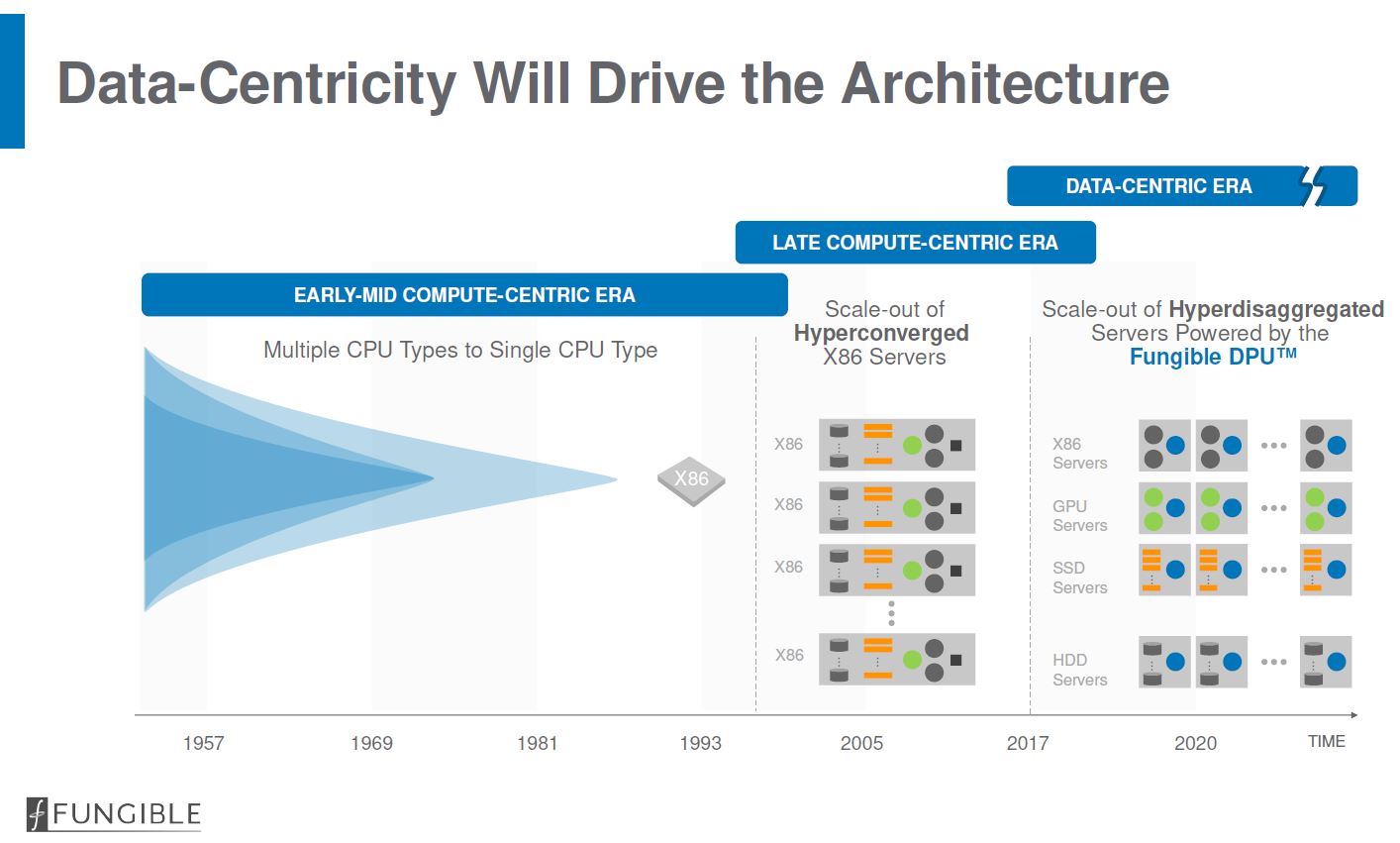
The idea of a data-centric era is a message many companies are using these days. For example, the Intel Data-Centric Innovation Summit happened on August 8, 2018 (8 is a lucky number in Chinese influenced cultures.) Pradeep’s view is of servers that are hyper-disaggregated. The view is that there are x86 compute servers, GPU servers, SSD servers, and HDD servers. In any event, these fundamental scale-out server types are designed for a common purpose: to make their most valuable resource available on the network. As that is the goal, the Fungible DPU can serve as the common endpoint.
Fungible sees the DPU as addressing the five root causes of data center inefficiency. All data center computation comes in via packets. Network, storage, virtualization, and security stacks are distributed via packets. As a result, there are more efficient ways to bring compute and data together and perform work than bringing everything onto x86 systems.
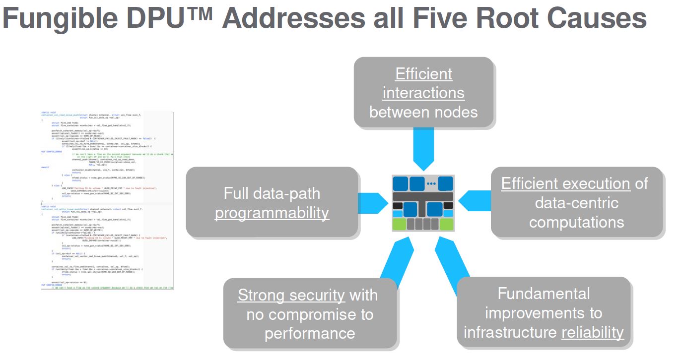
Enter the Fungible DPU that is focused on directing that compute.
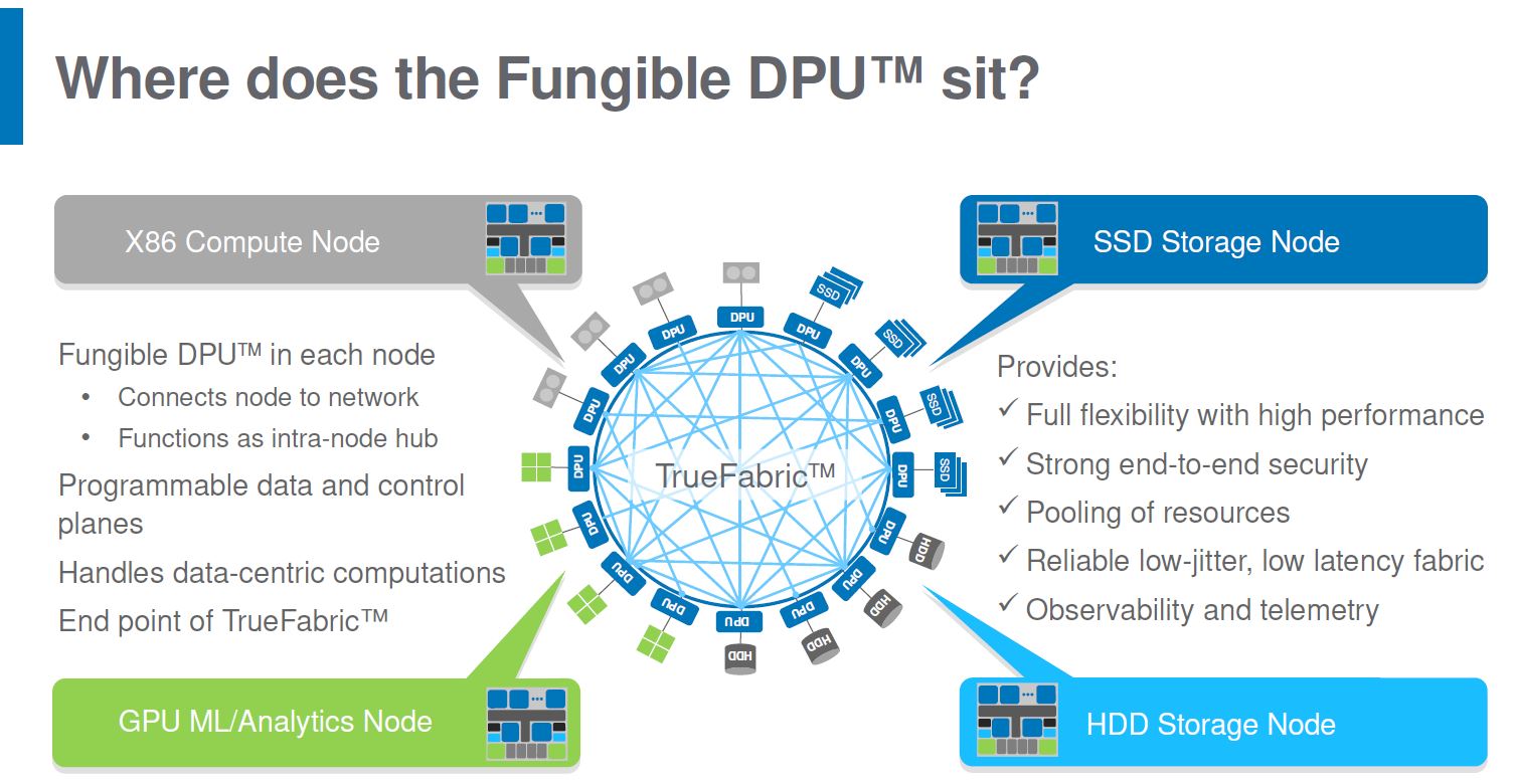
A DPU is essentially PCIe on one side and Ethernet on the other. For those four main hyper-disaggregated building blocks, the DPU provides an endpoint of “TrueFabric” which allows one to bring all of those elements onto a network. For those with networking backgrounds, everything ends up coming back to networks with connected devices which is different than talking to those who had careers that started building bigger CPUs or GPUs.
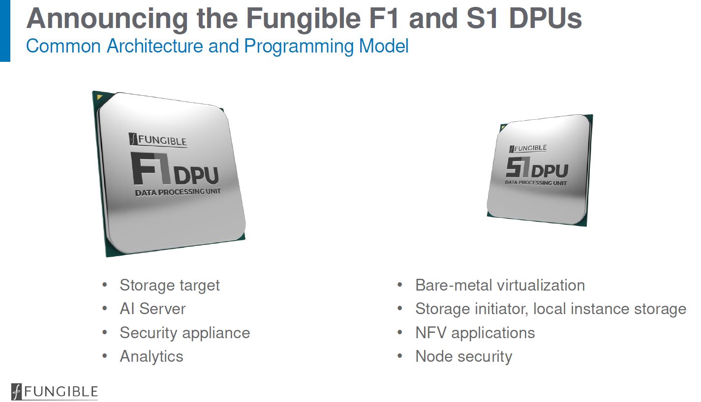
The talk focused on the Fungible F1 DPU, but the company also announced the S1 DPU. The S1 DPU is designed for storage and to be placed on a PCIe card.
Hopefully, we get to have some hands-on time soon, but it is great to see a family is forming.
The Fungible F1 DPU
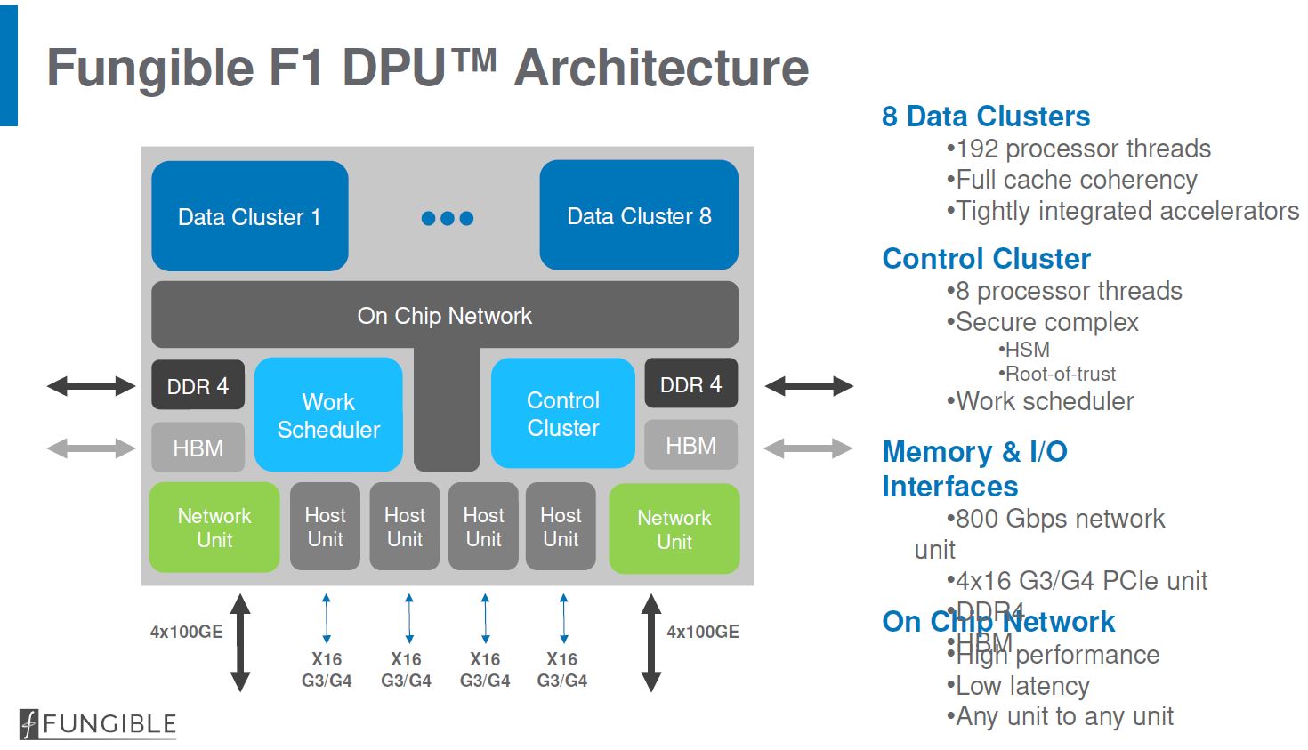
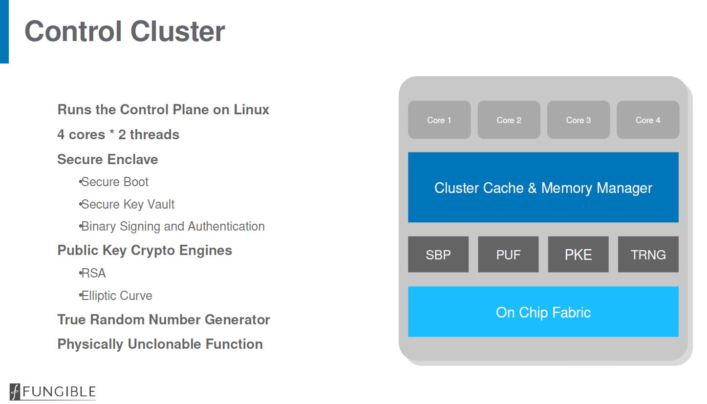
Here is the high-level architecture for the F1 DPU. One can see a set of eight data clusters that are split into 8x 24 thread clusters. There is a control cluster for the security and control plane of the chip. The F1 DPU has 800Gbps of networking such as for 8x 100GbE. There are 64x PCIe Gen3/ Gen4 lanes split into four x16 hosts. That is similar to what we will see on the Intel Ice Lake-SP Next-Gen Xeons.
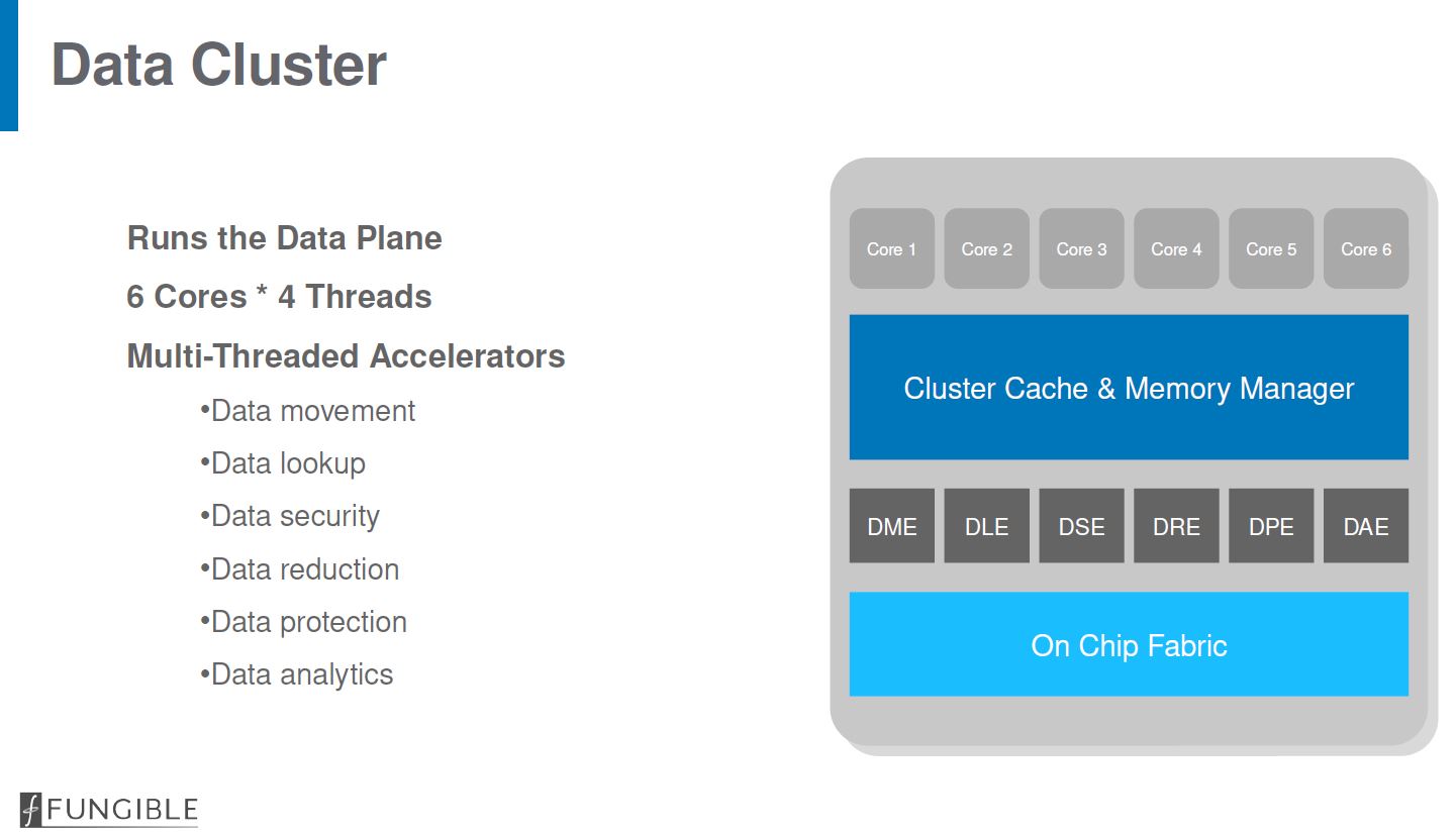
The data cluster is based on MIPS cores with SMT=4 designs. That means each data cluster has 24 threads plus their local cache, accelerators, and connection to the larger chip structures.
The system has both 8GB of high-speed HBM2 memory as well as DDR4 ECC memory controllers. It can also support NVDIMM-N which is very interesting as that effectively adds a persistent memory capability at the DPU level.
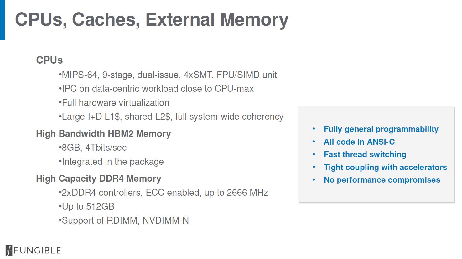
Fungible was asked about the MIPS use versus something like Arm. At HC32 the answer given was that very little is uniquely MIPS, but that was the best fit at the time.
With most systems these days, there is the main complex that does the primary work. There is a smaller complex that does work such as running the control plane as well as providing platform security. The DPU F1 follows this model.
On the networking side, there is a total of 800Gbps of networking onboard. One observation offered was that as servers move to have pipes with 200GbE and 400GbE each, having a server use its traditional cores for the TCP stack makes less sense. Instead, offloading this work to a DPU is a better option. We will quickly note here that offloading TCP, crypto, and other similar functions from expensive x86 cores is also behind the general SmartNIC trend. The DPU is aiming for more functionality than the basic SmartNIC model but that is a common theme.
Each PCIe controller can be an endpoint or a root complex. As an endpoint, it can connect to Intel Xeon or AMD EPYC CPUs and present itself as a device. The DPU F1 offers hardware virtualization features such as SR-IOV. Having a root complex means that, for example, one can connect devices such as GPUs, NVMe storage, or other controllers directly.
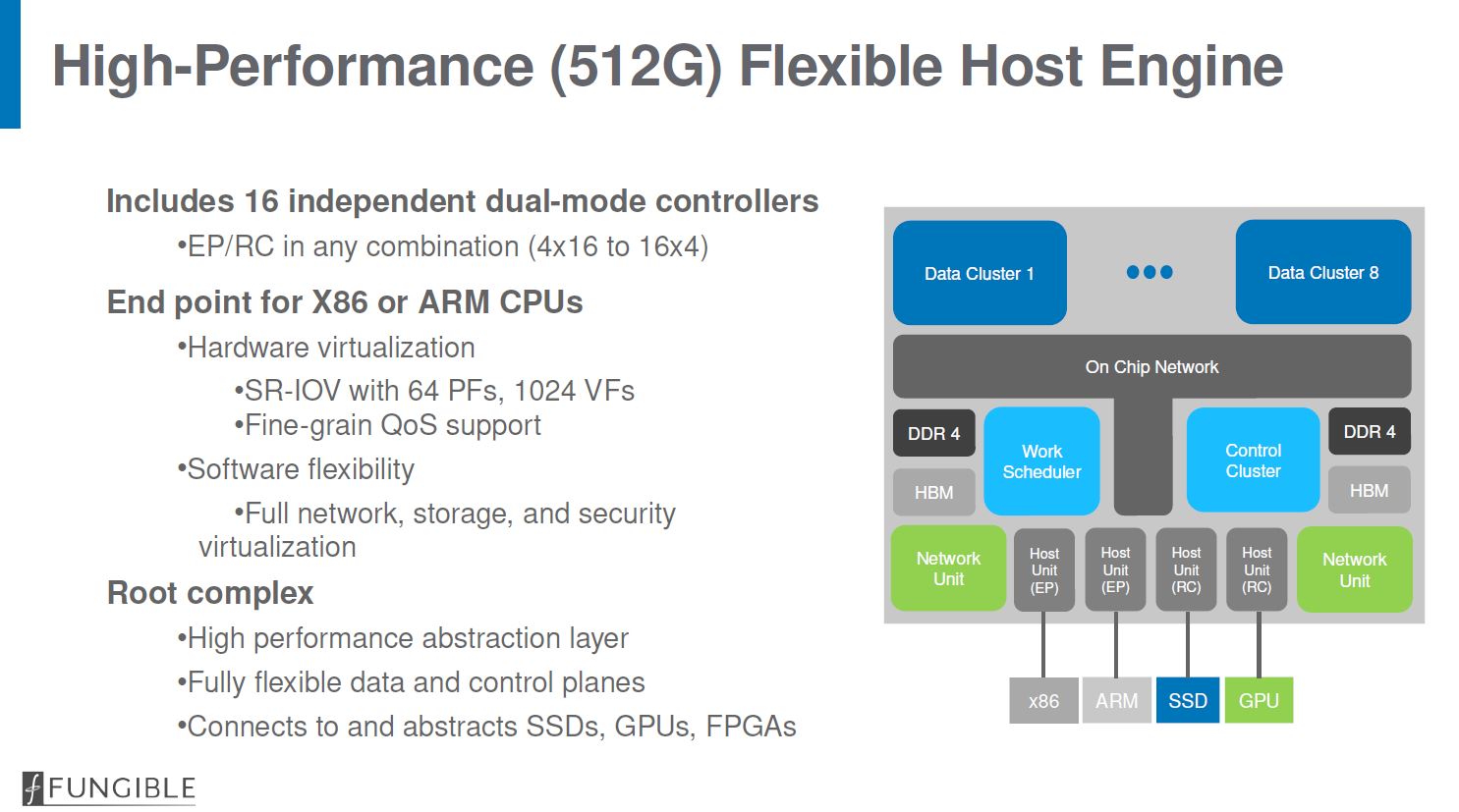
With this design, the DPU can connect all of the first order hyper-disaggregated server types (CPU, GPU, NVMe, and HDD) to the network.
Final Words
We are going to let our interested readers look into the programming model. At the same time, the impact of this model is important. If a DPU model is adopted in a data center, then the network carries data to and from and often can translate that data for transport and processing, even if it is not connected to an x86 CPU. To get to true disaggregation, speeds to individual nodes need to continue on a rapidly increasing path. 25GbE/100GbE and NVMe storage has made technology such as NVMeoF viable. Moving to higher-speed networks and peripherals requires that we re-think how we attach devices and compose devices on a network.
One can see a massive amount of research on this. We are seeing similar messaging from Intel and Xilinx on the FPGA side, and even the Mellanox EGX is moving in this direction. The big question now is, what will be the architecture and model that we, as an industry, adopt.


I can see from the dearth of comments on this article that it wasn’t just my head this has gone over :-)
So is this chip going to live on some kind of uber-NIC in a server/switch/router/whatever, or would it be central to some new kind of standalone host?
@Grimesey Sounds like the latter – this is designed for endpoints on the network, not the switching fabric. The article describes a vision that doesn’t have x86 processors on the nodes. They run Linux on the control plane, so maybe that has enough horsepower to run a storage server?
Not sure how this works with the hyperconverged trend. You pay for the disaggregation of resources, and simply packing nodes full of compute, memory, and storage and then virtualizing the spare capacity is cheaper (at least for SMB’s)
Comments are closed.