Confusion on What is Hacked, the CPU Perhaps?
While Bloomberg’s paragraph we just analyzed is rife with inaccuracies on the BMC attack, earlier in the article it was called a CPU hack. Here is the paragraph from the article we are going to analyze:
In simplified terms, the implants on Supermicro hardware manipulated the core operating instructions that tell the server what to do as data move across a motherboard, two people familiar with the chips’ operation say. This happened at a crucial moment, as small bits of the operating system were being stored in the board’s temporary memory en route to the server’s central processor, the CPU. The implant was placed on the board in a way that allowed it to effectively edit this information queue, injecting its own code or altering the order of the instructions the CPU was meant to follow. (Source: Bloomberg with emphasis added to highlight key points for discussion)
When the article described the hack, as discussed earlier, it utilized a BMC vector. Since we established that the chips, if they could exist (more on this later), would simply alter the BMC, then the instructions would be downloaded (they could not) and attack the CPU complex from there.
Key though is the language that the implants in the hardware were acting on the CPU’s temporary memory. We established in our first piece, Bloomberg Reports China Infiltrated the Supermicro Supply Chain We Investigate, that the hardware implanted does not have the pin count nor the processing power to perform this interception. Here is a dual Intel Xeon E5 V3/ V4 platform from Supermicro from the era in question.
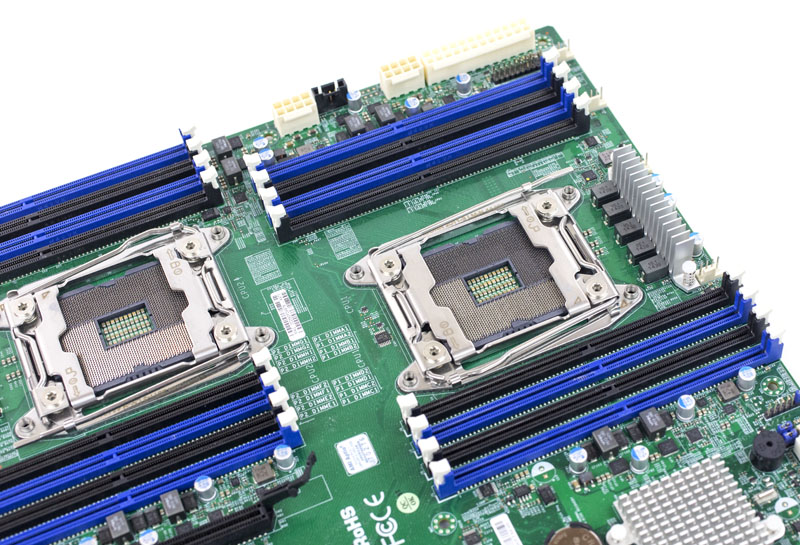
Note that RAM to CPU communication happens over thousands of pins. Each CPU has 2011 pins for communicating with the rest of the server. RAM pins take up several thousand of these channels. Note, in current generations, the 2011 pin sockets were replaced with 3647 pin sockets (and more for AMD EPYC.) Memory locations have been largely randomized for many years. This communication also happens at relatively high clock speeds, so keeping up with the bandwidth is a challenge for even CPU designers. There is no way for a small chip to attack the “temporary memory” (RAM) to CPU communication.
When we authored our original piece, we also looked at the feasibility of the SATADOM, a local OS storage, interface. Readers pointed out that the small SSD is not considered “temporary” storage since it is persistent. Attacking persistent storage or add-on cards would present other challenges, but this is between the motherboard’s temporary memory and the CPU.
Even if Bloomberg’s report mistakenly misused CPU in this paragraph instead of BMC, the BMC RAM as temporary storage is troublesome. Generally, BMCs have a single RAM package. Here is an example of a PCB without a BMC and its associated RAM package and flash storage set:
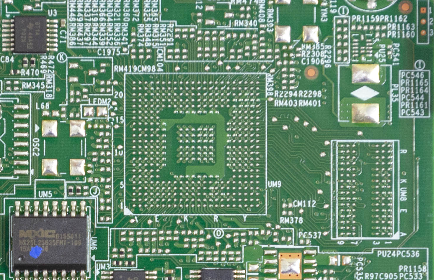
There are a few takeaways. First, in a chip the size of what Bloomberg Businessweek depicts multiple times, one cannot monitor dozens of data pins and traces coming off of RAM (right-hand set of pads for package placement) to inject code. The chip would need to be significantly larger to have the pin count to monitor any RAM temporary device.
Computers also have on-die cache memory, but Bloomberg stated that the hack happened at the motherboard level, and on Supermicro, not Intel hardware. Inserting traces into a modern chip package after it has been fabbed is essentially impossible given today’s technology.
Bloomberg cited “two people familiar with the chip’s operation” but there seems to be a disconnect between its description and how such a small device has the physical pin space, let alone the processing power to monitor so many high-speed pins.
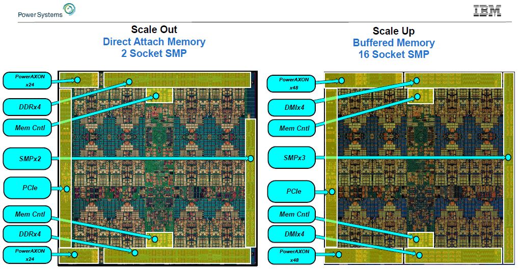
Intercepting temporary memory of a modern CPU via a motherboard component is not easy. If you look at, for example, the IBM POWER9 DDR4 memory controllers, an enormous amount of die space on a large chip is used to deal with memory. A large number of pins and high-speed signaling make it unlikely that such a small chip could do the job. Just the die area IBM, Intel, Marvell/ Cavium, AMD and others use for DDR3/DDR4 connectivity and processing is larger than Bloomberg’s alleged device both for silicon size and pin counts.
A Quick Note on the Ordering or Injecting
The last part of that passage we wanted to discuss briefly:
The implant was placed on the board in a way that allowed it to effectively edit this information queue, injecting its own code or altering the order of the instructions the CPU was meant to follow. (Source: Bloomberg Businessweek with emphasis added to highlight key points for discussion)
Many parties such as Apple and Amazon have pointed out that they believe that the Bloomberg Businessweek reporting staff was confused. We have had readers suggest this “altering of the instructions the CPU was meant to follow” sounds a lot like the Spectre/ Meltdown (many vendors) or L1TF (Intel) vulnerabilities. This is vague enough that we will let our readers draw their own conclusions.
The “or” in this a huge statement. In order for this statement to be correct, the implant chip itself must have logic built in to execute one of two different commands. This sentence says that the “implant… placed on the board… to effectively edit this information queue” in one of two ways. This paragraph is talking about the CPU, a term of art and something that is labeled as such on every server motherboard. This is not talking about the BMC as the BMC discussion that we covered above was later in the article. Based on what is in the article, this is attacking CPU to temporary memory and the BMC. If it is simply a BMC hack, it would be an implant on the board attacking the BMC, not a labeled term of art, the CPU. Perhaps this is more confusion, so we will assume that this is a technical error by the Bloomberg report to help “dumbing the story down” for non-technical audiences.
That “or” presents an implication. Assuming such a small chip could be placed on the motherboard in a way that attacks the CPU to temporary memory communication, this chip needs to store its payload, it needs to communicate across motherboard communication pathways, and make logic-based decisions. That is a lot of functionality for a small IC package. Therein lies the next challenge.


These Bloomberg guys are shady. I know this isn’t STH’s focus, but you’re doing a great job on this line and you’re the server expert. That first page was completely damning. There’s no way you can look at their statements dissected like that and say their story is completely true.
If I wanted to read a fictional novel, the Bloomberg guys are better writers than you so there’s that.
It’s refreshing to see a competent analysis. Bloomberg’s story is total BS and is a smear campaign.
I design chips for a living. Your list of leading process companies that could do this should be shortened. Only TSMC, Intel, Samsung, and GloFo can be the sources of these chips for leading nodes. You’re right, they don’t have the die area in those packages to make these chips on 14nm+. You left out the critical element that they also need to cut the wafer, package the die so it can be used in manufacturing. That takes space that Bloomberg’s representation fails. Maybe you mention it, but there’s no way to make something that small today in 7nm let alone in 2015 in 14nm.
I wouldn’t call this riveting, but your technical parts are spot on. I now think there’s no way Bloomberg is right here. An investigation must happen and heads at Bloomberg need to roll. Your first page alone shows that their editorial staff whiffed since you’re right. Drives aren’t on if the server is off. I didn’t catch that when I read theirs but it’s a good catch. Your BMC networking is simplistic, but it gets the point across. Every admin should know this.
GREAT
The TL;DR since this is forever long:
p. 1 – Bloomberg got basic technical details flat wrong in its piece.
p. 2 – Bloomberg f*d up simple stuff like keeping the BMC and CPU straight in their article.
p. 3 – Bloomberg’s chip functionality, size, and rationale don’t make sense and there’s only 4 companies that could have produced the chip.
p. 4 – Anyone Bloomberg has publicly relied on says they’re a bunch of confused individuals. The ex-Supermicro employees are used to paint an almost racist picture of the company. — I’m reading between the lines here but that’s the impression I got on my first read of the Bloomberg article too.
p. 5 – SEC needs to investigate. Lawsuits need to happen. Bloomberg may end up as an Apple brand after this is over because they’re standing by a false piece.
GREAT
What happens when the world’s leading server expert shits on your crappy reporting Bloomberg. #dunked
We’re only running about 100 servers. Setting up a dedicated management network is the first thing we do and everyone blocks egress on their management network. That’s spot on.
Is coming from a different viewpoint or am I not reading this right? Their premise is that in order for the article to be correct, it must be 100% correct. I think Bloomberg has a collection of half truths.
I didn’t see you include any verbiage on the BMC’s PECI connectivity to the cpu– that might be an interesting way of injecting code. For the record I do not believe this hardware hack is real, but the PECI angle is interesting.
It sounded to me like Bloomberg were maybe referring to an attack on the boot code stored in a QSPI flash package. This would be something the BMC has access to in order to update (right?), and the CPU also has access in order to boot from. The limited number of pins and slower speed of SPI drastically reduces the HW requirements for an implant.
I *know* that preventing attacks against firmware is a major concern amongst hyper-scale/cloud companies. See the recent NIST 800-193 “Platform Firmware Resiliency” spec.
I’m not saying Bloomberg is right, just curious if the SPI boot ROM angle has been looked at.
Seph I’ve done this on smaller boards. If you put something in a PCIE path you’ve got to reroute the PCB traces potentially through layers and moving other wires as well. PCIE traces have length requirements. So do RAM traces. There’s a picture of the RAM traces in the cover image to the article. If you’re looking at the zig zag pattern that’s to get the right trace lengths. This article could have done more explaining how hard it is to change anything in PCB. These server boards have many layers and are large. Signal integrity is a challenge.
Isn’t ROM persistent not temporary memory? If it was a ROM attack, the Bberg article wouldn’t say temporary memory. I think they’re constraining themselves to the article’s description. Their first article on this says they believe hacks exist so I’m reading this one as only related to what’s described in the article.
Also, if I were doing this the chip would not have flash, just a mask ROM with code and internal SRAM for data. Heck it might not even be a processor, it could just be a state machine primed to trigger on seeing a certain pattern. The payload would then be delivered from the on-chip ROM. Nothing about this requires a highly advanced node.
FWIW I find Bloomberg’s reporting highly suspect, but this is an area of security that interests me.
Walter: Seph meant PECI, not PCIe. That was not a typo. See https://en.m.wikipedia.org/wiki/Platform_Environment_Control_Interface
Also, the temporary part would be that the actual flash chip is not reprogrammed, you are just modifying the instructions as they are delivered to the chip’s internal SRAM. If this is what Bloomberg was trying to describe, they did a terrible job of it.
Do BMCs boot from external SPI flash?
Too much reading after 5 pages Evan. PECI this is a better reference since they’ve showed Xeon systems of an unknown vintage https://www.intel.com/content/dam/www/public/us/en/documents/datasheets/xeon-e5-v2-datasheet-vol-1.pdf
It’d be a wild hack if that’s it as it doesn’t really sound like what Bloomberg’s saying. If it were, you’d say it was in the environmental control right? I’d have to think what’s possible there as I thought PECI even has ECC for signal integrity.
This article touched on the issue with a simple hardware altering storage with low processing power. If you’re altering the flash chip it’s still storage not memory.
It’s intriguing, but it isn’t what they described. I’d like to think we can all conceptualize types of hacks, but once they put it in writing, the time for concepts is over.
Herein lies the issue. You’re trying to use logic and technical reasoning against a story that’s make to be anti-China and made for people that think being techno savvy means operating Face Time.
I disagree with your analysis of Bloomberg’s inaccuracies, your analysis being inaccurate as well :
– Assuming the BMC is compromised, you cannot prevent it from using the shared NIC. So if the shared NIC has egress connectivity, a compromised BMC can get egress connectivity. The BMC can also mimic the normal traffic to evade any kind of pattern-based detection. The only way to make sure BMC has no connectivity is to cut egress connectivity on the dedicated port AND the shared network port, period. Still, I assume those 30 companies would never give egress connectivity to any server.
– Your point about accessing storage on “turned off” devices is moot. BMC can power the server on, do its thing, then turn the server off. No one will notice.
You’re right about physical interception of the “temporary memory”. However, the BMC being connected to PCI-E, it can use DMA to e.g. change boot code in memory right after it was loaded from disk and before it gets executed.
In the end, I believe you’re under-estimating the impact of a compromised BMC.
Olivier if the server is off it is not on. You’re changing parameters if you say the BMC is turning it on. You’re also right that if Bloomberg had written their article differently, they may have been right, but it’s not clear. Once it is on, it isn’t off.
We use Microblades and they’ve for 1G and 10G ports along with management. Nobody is using the onboard 1G ports for anything other than provisioning networks that don’t need egress either.
Compromised BMC’s are an industry problem. I’d agree with you there. The more functions that you’d assume the hacking chip has, the more storage and processing power it needs making it less likely to be small.
@Trevor Dedicated network cards won’t necessarily protect you because the BMC chip has DMA capability.
It can also pre-empt firmware loading on the main CPU or modify ring 0/SMM/ME memory after boot so any traditional security (including. IOMMU) can be bypassed.
The only commercially-available way I can think of is by combining a signed firmware image with TPM metrics and RAM encryption (AMD SEV/Intel SGX). Though the BMC can probably still intercept the traffic to TPM.
“The implant was placed on the board in a way that allowed it to effectively edit this information queue, injecting its own code or altering the order of the instructions the CPU was meant to follow.”
I’m not saying a BMC hack isn’t bad. The verbiage says that the implant itself not the BMC is doing the work in this line. This doesn’t say that the implant compromised the BMC which then works on the CPU.
BMC hacks have been around for over a decade so it isn’t like people are failing to take precautions.
If you’re doing BMC hack, you’re better off putting it on a USB and having it installed after manufacturing when it’s going through logistics to installation.
Don’t know if Bloomberg’s article is fake or if the journalist didn’t get it, but if I wanted to do such attack, I would target the small (Q)SPI memory which stores the BIOS (it’s usually 1-8MB). Intercepting the BIOS loading and injecting couple of KB of memory in the microcode memory would be possible with a chip the size described in Bloomberg’s article.
And once you are in the microcode, I don’t think there is anything you can’t do or access… but I’m no expert.
A quick search shows it’s possible to fit 128KB in 1.5×1.5mm package: http://www.gigadevice.com/press-release/gigadevice-introduces-low-power-spi-nor-flash-memory-with-uson8-package/
A direct system BIOS attack through SPI isn’t really going to happen right? They’re “capable of doing two very important things: telling the device to communicate with one of several anonymous computers elsewhere on the internet that were loaded with more complex code”
Hitting the system BIOS to stop authentication checking, maybe that works, but you’re now going at the CPU not BMC. You’ve still got to go after the BMC first.
Attacking the BMC’s flash storage might work, but you’ve also got to contend with the software images changing as new firmware gets released, signaling changes if you’re in the traces, and others. That USON8 is only 1.5mm but you’ve got to add in networking, a controller, and processing power. The linked USON8 is 1.5mm in 2018, not in 2015 and you’re talking about having more functionality not less in older generation manufacturing.
This article missed the point that it’s going after the Linux OS on the CPU and the BMC. It’s also needing to download additional payload right? The more complexity you’ve got the less I can see this being made.
Only way this works is if someone made a chip that attacked the BMC that would not get stuck after a firmware update. I know at least some companies have their own custom firmware, so if you’re attacking the firmware at a low level you’ve also got to get the firmware image. Cloud guys usually don’t use the full stock Supermicro or other firmware since they gut what they don’t need. You’ve also got to evade any firmware and OS checks that the cloud guys have. This article missed those points.
They’d then need to get around typical egress issues. Then they’d hit a C&C server that would bring back code to push to the main server. For the DMA vector they’d need the server to boot after the C&C payload hit to attack the rest of the to get to a low level of access.
You’re still better off with a USB drive that can just attack the flash at the end of factory testing or into logistics since there isn’t a trace and it’s faster to react to systems changes.
If you go hardware, and some software part is altered, you’ve got sitting duck hardware for someone to investigate and that hardware can be obsolete. You’d then need to update your chips or re-fab. Motherboards also go through spins so you’d need to find a way to make it all work with different components.
I don’t think this analysis is perfect, but it at least lets us all define just how narrow the opportunity to pull this off. If we’re thinking of this now, then the companies and government officials who Bloomberg says have known for years it’d be easy to find. If it was easy to find the recent post investigation Apple-Amazon-Supermicro statements are false.
They still can’t read the most sensitive data on a server that’s turned off since SSD’s don’t have power. So the story’s still buggered there and the rest relies upon some really big leaps of faith of things going right for it to even work. Even putting on my tinfoil cap for this I’m wincing at how crazy those leaps are.
For a server review site, and not a site that does this sort of content, pages 1,3-5 are pure gold. 2 you could have gone the SPI route but Bloomberg didn’t call it out so we’re all “just guessin’TM” here. I take pg.2 as it’s narrowing possibilities.
Enough here that there’s no way Bloomberg is 100% right. I think they heard of some different attacks and tried piecing something together. There’s something to be said that they couldn’t write about it clearly enough or with keywords like DMA or SPI that we’re all not sure how it really worked.
STH REVIEWS SERVERS. WHY CAN”T YOU GUYS SHOW US THE CHIPS USED IN THE BLOOMBERG ATTACK??????????????? WE WANT TO SEE THE REAL CHIPS. PLEASE UPDATE THIS
Great job STH. Excellent article, everything is nicely explained, even non-technical persons can understand what’s going on.
I am actually really, really mad about all this. This is not the first time that Bloomberg is hurting other companies with bullshit stories. They should be shutdown immediately and thorough investigation should be carried out. Supermicro, Apple, Amazon and other companies that are suffering from this should sue Bloomberg and take everything from them.
I am really pissed off!!! Isn’t it enough that we have real threats in IT world? We really don’t need this kind of stories going around.
Who would have a financial or political interest in seeing technology stocks suddenly drop in value?
Unlike the others, I like your analysis on 4 of the sources. Someone will trace and do better perhaps. Here’s my takeaway. If the Apple sources come forward, they’re going to have to contend with the investigation they know is going on now. Maybe the random web host can come forward. The only sources they’re using to support are government sources. They even cite an intelligence official who studied SM’s business model. What’s that job? Water cooler jockey?
If it’s all supported by government officials leaking classified data, they go to jail if they’re named without air cover. That air cover from senior FBI and NSA says it isn’t real. So their bosses won’t give air cover. If someone comes forward now admitting to leaking classified data, that’s jail or a dig at their boss or both.
You’ve also left out another salient point, there’s another 27 companies who were notified and not named. Where are their people coming out to support this?
There’s too little detail in their article and they’re now on an island. We can all say it’s maybe possible, but Bloomberg said it happened and there’s some human side holes to fill now not just the technical parts.
Small type on page 5- Supermicro is misspelled Sueprmicro. Or perhaps this was a freudian slip :)
Only need this one question answered: Since it caused the SMCI stock to drop more than 40% in one day, is the related paycheck-collectors.gov still hibernating with their paychecks automatically, directly deposited?
It’s all about manipulating stocks, it happens to Apple more than others.
While the original Bloomberg article isn’t great on details, I believe this chip as described is actually something that could exist and would actually be cheaper and easier to implement than most people think. While I have zero knowledge of the actual exploit as implemented, here is how I would implement it:
The trick is to make the chip do as little as possible and be just a first stage bootloader for the exploit. All heavy processing and IO can be provided by the BMC. The BMC controller stores it’s firmware in an external SPI flash chip. Placing a custom chip on this SPI interface would allow for code injection to the BMC. While the firmware does change, the BMC really runs a full blown embedded Linux install. The boot process for Linux is fairly stable so rewriting a function or two early in the boot process to add additional functionality and changing the program’s vector table wouldn’t be that difficult and would have a very high chance of not changing for future firmware revisions.
The injected code would really only need to serve one purpose. That would be to connect over the BMC’s network connection to the remote C&C to download a larger payload. While the dedicated BMC network port would be connected to a separate management network, the BMC has access to share one or more additional network interfaces on the server. This is used so IPMI can be used even if a separate network connection is not used. This is something that you can not get with a software IPMI exploit and the entire reason this attack would be worth doing in hardware.
Once the BMC is taken over, it is possible to take over the rest of the system. Since the server is not designed to treat the BMC as a threat, it is able to essentially take complete control of the server. One of the interfaces provided by the BMC is a PCIe connection to the system. PCIe has built in DMI access. This would allow rewriting program data that the article referred to.
Now how much would something like this cost to implement? A few hundred thousand dollars. By limiting the actual hardware to just being a bootloader for the rest of the exploit and hanging it off of a relatively speed and low pin count interface like SPI, it is possible to build the chip in an older cheaper process. Something like a 180nm process would be cheap to build the chip in and would allow adding enough logic and ROM storage for the exploit in a 1mm^2 package. Compared to the exploits listed in the leaked NSA’s ANT catalog, this really does not seem to be that far fetched and considering the capabilities afforded, the exploit actually seems very realistic.
Andrew we’ve done work trying the same method and you’re greatly oversimplifying it. If you’re targeting these guys, there’s a whole host of custom things they do that you’d need access to their production HW+SW+FW before you’d be able to do the attack and it’ll be different for each customer. You’ve also missed the networking claimed and there’s no way you’re going to do this on 180nm in a 1mm^2 with all of the functions Bloomberg lists. Sorry.
I think this story was a plant by Bloomberg to crowd source their way out of the problem. They’re trying to reach for anything to help them in litigation.
Yes, I agree there is no way this chip implements it’s own hardware network connection. There is no chip you could build that small with integrated networking. The article stated “networking capability”. I don’t think this means hardware networking, but using the BMC’s existing network access to network with the C&C.
There is also zero reason for the hardware to care about actual software running on the system. The exploit is entirely built into the BMC, so the only software that can change to defeat the chip is the BMC’s firmware. How many companies are writing their own BMC firmware for off the shelf Supermicro motherboards? Once the connection is established with the C&C, that is when a remote attacker can then exploit the rest of the system. Since they have full 2-way communication at this point, analyzing the running software on the server and exploiting it is much simpler.
A tin-foil hat wearing coworker of mine suggested this chip could have “some other way of getting out without TCP/IP..you never know, state-funded attacks can be very elaborate” and let’s say for a second that makes any sense. Everything comes down to pulses at some point. Couldn’t someone throw an oscilloscope or some other means of analysis on a network port and look for /some/ kind of activity? If this chip were real…in reality, it’d have to be reaching out to something via TCP/IP and any number of network traffic monitoring tools would have caught strange behavior, right?
Comments based on what’s in the replies here:
– supermicro has a feature for BIOS flashing (system off) via BMC
– flashing the BIOS allows replacing the microcode
– 1g interfaces are often connected.
– supermicro is known to fall back to “shared mode” (plus, it’s configurable via OS)
– OS can also re-flash the BMC (if one has the endurance to deal with the shitty tools)
– BMCs crashes occur non-rarely once you got 1000s of systems. simply by normal bugs and issues. no way to detect malicious ones.
– BMC networks might not have egress to the internet, but are usually routed somewhere (C&C internal)
– BMC networks normally don’t surpress crosstalk, so side-stepping is not impossible.
– In the Bloomberg illustration the implant sat on a pin of the SPI flash socket (empty in illustration) for the BMC. Since most non-crazy theories here lean towards modifying SPI flash (i barely know how a BMC boots, will not try to make it sound otherwise) just nudging the BMC boot would be sufficient.
I forgot the rest I wrote before some ad triggered a page reload.
Level1techs made a nice video about this subject
Blather on all you like about what is possible and what is not when you don’t know the attack mechanism in detail. You can criticize others for being vague but you can’t fill it all in when the alternatives are nearly infinite.
‘
True hardware level attacks render all software and protocol defenses open to subversion. On the software side that is what makes root kits so difficult. Any fool who tries to say what are the limits of a root kit would be well advised to study the meaning of decidability (Halting Theorem). Hardware is interchangeable with software in frozen form until the electricity starts to flow in which case it is logically indistinguishable. Information and information processing is abstract not limited to only one physical embodiment. The rules remain the same for all cases.
I attended an RSA lecture over a decade ago where it was shown a seemingly random one bit arithmetic error not likely to be detected could be used to defeat large key encryption. Once you can compromise at the hardware level the floodgates are open, including defeating all the means to detect it in software.
What Bloomberg did not speculate on was the potential to tamper with CPU, GPU, and controller masks and resultant physical chips at the point of manufacturing. The threat is real and defenses virtually non-existent once the opponent has prior physical possession of the digital equipment. In China you have by far the most sophisticated and advanced cyber adversary on the planet. Americans including the NSA are drastically out matched. And the insiders know it.
That should be pause for thought rather than trying to show how clever you can be in what didn’t happen without knowing what did happen.
Rob DuWors, Andrew, Olivier, Evan, Seph – all spot on. This sth article views the matter as a server or network attack. Seen from an information view, or systems/knowledge/social/electronic/physical view, a hack such as the one described in Bloomberg’s story is par for a course in cyberwars.
Apple, Amazon and others have rightly called the story untrue – because they, the hack party and everyone else knows that the target is not the consumer/business data that is stored/transacted in the servers of these cloud service providers; the target is the belief of consumers and businesses that tcp/ip and all that it has begotten today is secure/private. All nations have all the incentive to get the networked world to subside a bit. This particular case was probably an amateur/trial shot. We live in information times, constructed using hard and soft wares, and everything wonderful and obnoxious is possible cross-border as long as there is tcp/ip and transistors.
What if there was a proof-of-concept board that the security experts were referring to and then Bloomberg exaggerated the story to say that the exploit was in actual retail products. I could see the Chinese creating a one-off board.
At least one article I read alleged that the chip might manipulate the actual BMC firmware via I2C or JTAG, which are both low-pincount access methods. This would resolve the size and pin issue, but would probably make the chip much more detectable, since it would most likely screw up operations after the first BMC firmware update.
…are registered Dimms connected to the BMC ? Why wouldn’t a memory controller be built into the buffer, to read contents of the memory and transfer back over the SMbus ?
The Bloomerg article is full of incredible detail and still missing the obvious….Maybe its a waste of time to imagine how to interpret the fantasy into something practical…
Comments are closed.