
Without question, the coolest technology at Hot Chips 31 is the Cerebras AI chip. While most of our readers may touch an AMD EPYC 7002 series chip in the next 24 months, it is unlikely you will get your hands on one of these. Instead of a chip being 1% of a 300mm wafter’s yield or less, Cerebras is going the other way. They are doing a wafer-scale chip. Not a one-quarter wafer-scale chip. This is the largest square chip you can make from a 300mm wafter on TSMC 16nm. In contrast, a NVIDIA Tesla V100, or an entire server worth of NVIDIA Tesla V100‘s look small in comparison. NVIDIA just lost its “largest chip” by a wide margin.
A quick note for our readers, we are taking photos, but the WiFi in the Stanford auditorium is slow so pictures will be added as uploads become possible.
Cerebras Wafer Scale Engine AI
Cerebras is doing something truly different here. The setup is simple. Going off of a physical piece of silicon and through PCB is slow. Instead of doing that, if you can use a single giant piece of silicon, you avoid the interconnect and memory latency. Just to give you some sense of how big this is, here are the key metrics:
- 46,225 mm2 silicon
- 1.2 trillion transistors
- 400,000 AI optimized cores
- 18 Gigabytes of On-chip Memory
- 9 PByte/s memory bandwidth
- 100 Pbit/s fabric bandwidth
- TSMC 16nm process
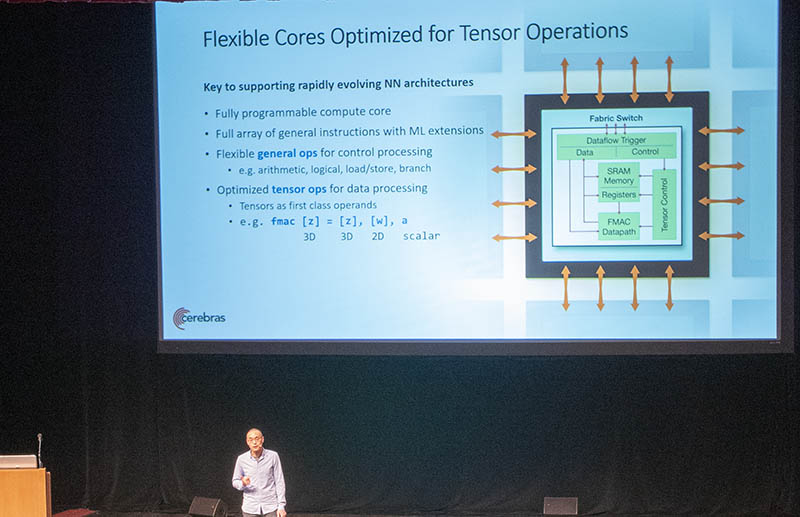
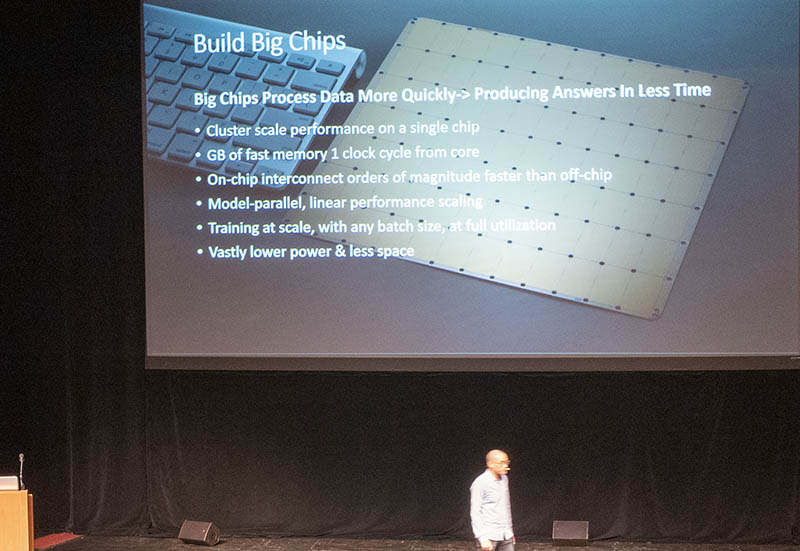
With all of that silicon space, Cerebras has a giant chip designed to handle tensor ops and move data around efficiently. Onboard SRAM memory in the enormous array of AI cores with the high-speed interconnect has a simple goal: turn what would normally require an entire cluster of servers into a single piece of silicon.
Frankly, this approach makes a lot of sense. Silicon interconnects use less power and has lower latency than going through PCB and external cables at high speeds. While the chip itself can be more expensive, having one giant chip that removes the need for network fabric and say, 10+ servers to house the single Cerebras chip worth of AI silicon is an enormous cost. In this design, the power of the individual chip will be high, but should be dramatically lower than the cluster of systems it replaces.
There are a number of challenges that the company faced and discussed at Hot Chips 31 (2019.)
Cross-die connectivity
One of the key challenges the company had was how to handle connectivity across the entire die. Normally, there are spaces called Scribe Lines, in manufacturing to give space for cutting and testing. If you make a giant wafer-scale die, you need to run wires across these lines.
Yield
While AMD and Intel are moving to multi-chip packaging (or what Intel calls glued together chips), to make bigger silicon complexes while maintaining yield. Cerebras is going the other way with a giant chip. As a result, defects are expected on every wafer and therefore every chip. The Cerebras Wafer Scale Engine design expects these defects and has extra cores and interconnect wires to handle these defects.
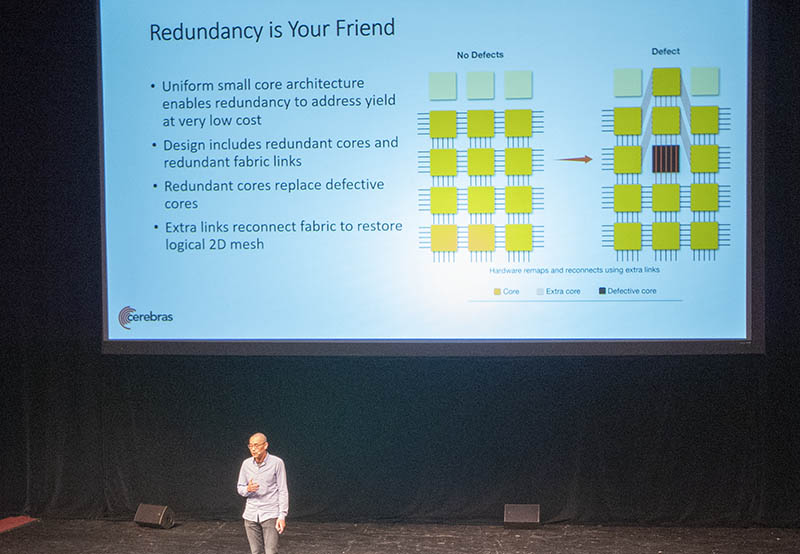
Using this approach, Cerebras can be “defect tolerant.” While NVIDIA is focused on getting smaller perfect or near-perfect dies, Cerebras designed the Wafer Scale Engine to have multiple defects.
Thermal expansion
As the Cerebras Wafer Scale Engine runs AI models, it consumes power and generates heat. Heating materials can cause them to expand. In large solutions like this, that can create issues, just as it can for highways you drive on.
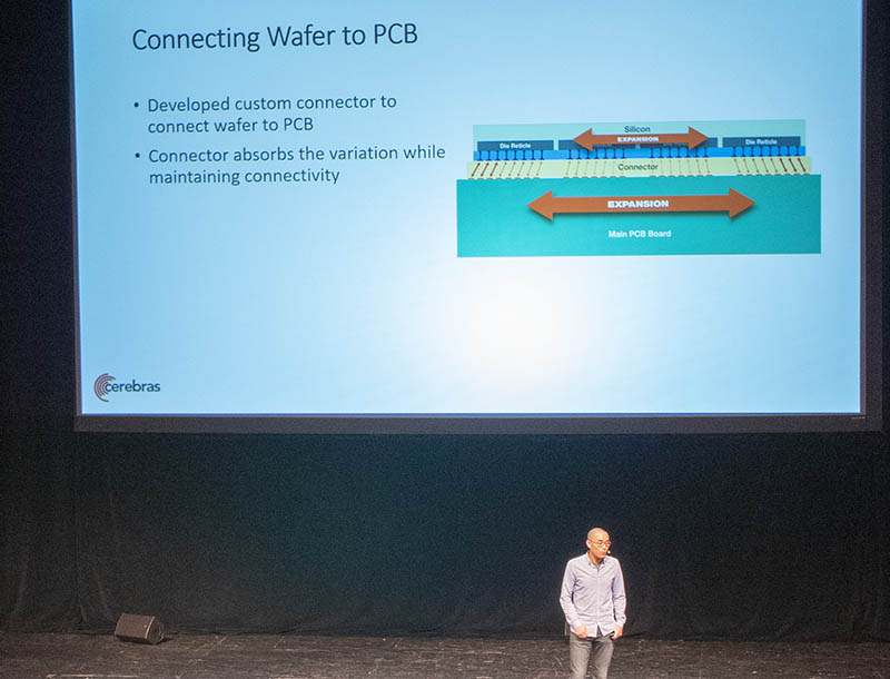
The giant silicon wafer and PCB expand at different rates which could cause damage. Cerebras is using a connector layer between the silicon and PCB to handle this mechanical stress.
There is also a cold plate atop the silicon to transfer heat away from the wafer chip.
Package assembly
Putting the silicon, PCB, connector, and cold plate together was a challenge.
Traditional tooling did not exist since this is a piece of silicon so much larger than anything before it. The company had to develop custom tooling to make this work.
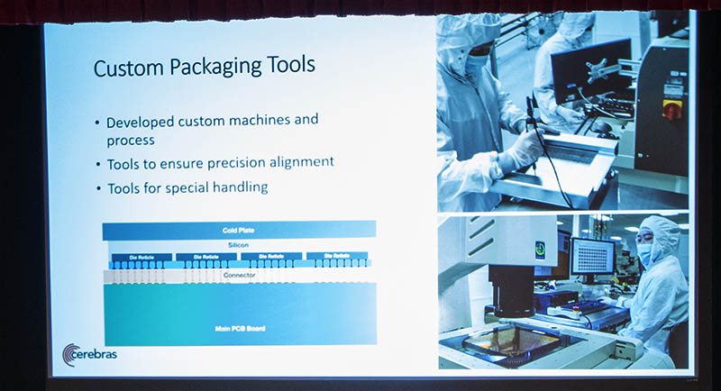
Specifically, the company had to solve for handling and alignment of the different components.
Power and cooling
Since the Cerebras Wafer Scale Engine is so big, it cannot be cooled via air and power cannot be delivered using a traditional planar delivery method.
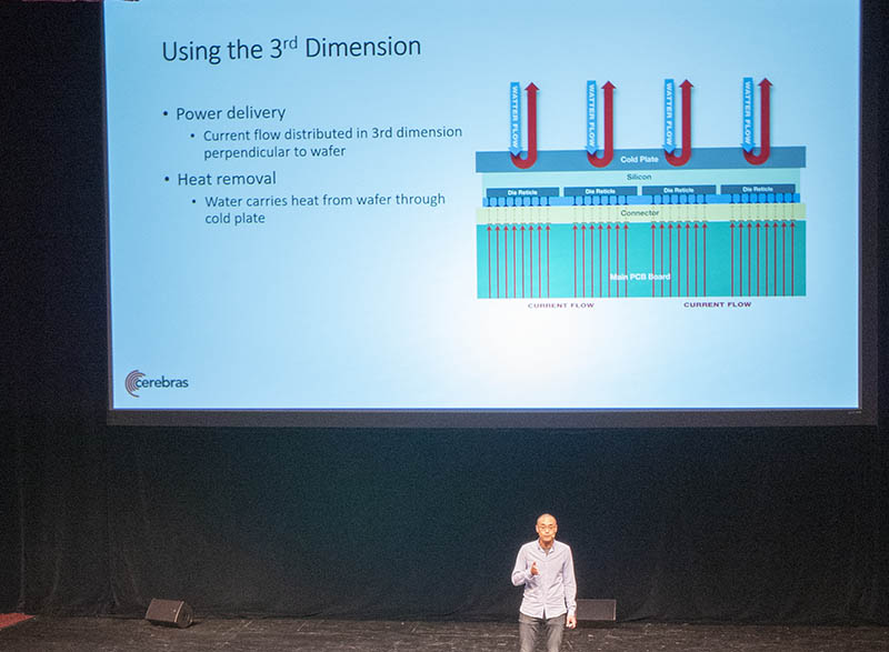
Instead, the company had to do a more direct perpendicular power delivery along with water cooling (across the cold plate.)
Final Words
From an engineering standpoint, this is an awesome achievement. For the industry, this is a potentially awesome capability. It shows just how hungry the AI industry is for more compute. Truly novel solutions like this stoke the entire industry. If you had any doubt that AI is driving the industry, this is now the prime example. Moonshot engineering efforts like the Cerebras Wafer Scale Engine are what will give the bigger players and smaller startups the courage to make big bets and think differently.


 the Cerebras Wafer Scale Engine stole the show as being an AI chip so large that it is the biggest chip possible on a 300mm wafer)
I saw someone somewhere claim that this is a 15 kW chip. The mind boggles. That’d be what–4x full 30A 208V circuits just to provide power for the one chip and a bit of redundancy?
wow, the only space where I’ve seen whole wafer designs before is image sensors. This is an entirely different level of crazyness.
This is 50x the transistors and 50x the size of the largest nvidia chip, so 50x the power would make sense, that’s indeed close to 15kW.
The resurrection of the 450 mm wafer is on it’s way…
How it’ll interface with external memory, network etc?
What’s the expected cost of it – 100K$? 200K$ ? more?
Holy Sh**!
Yeah this isn’t going to use close to 15KW as it would melt the silicon on this squared volume.
I’d love to see pictures of the finished deployed processor in a rack mount case. I’ve an image in my mind of this rectangular metal chunk ~22 cm on a side with a few hoses and IO connectors. Some sort of real Star Trek “processor”.
@Igor – I think the idea here is that with massive amounts of local memory, you can preload the dataset without needing the same memory bandwidth you would for GPU’s. That saves a lot of pins.
@Minelleke – It sounds like they have a unique cooling solution, perhaps integrated heat pipes? Regardless, by using liquid cooling, they are not limited by air path distance, and with integrated heat pipes, heat spreader, and a solid cooling block, they can avoid hot spots and provide adequate cooling.
Nothing about clock speeds, so I suspect they’re trading off the sheer number of transistors for speed, effectively underclocking and under-volting to the point where they meet heat density goals. Keep clock speeds down, memory bandwidth up, and it’s a better balanced anyway.
I would not be surprised if it’s running <1Ghz, built on low power process, and then tuned below theoretical limits of the process.
Professor: Divide and conq..
Cerebras: Yes.
Comments are closed.