At Hot Chips 2023, we learned more about the AMD Versal Premium VP1902 FPGA. We recently covered this in AMD VP1902 is Leviathan FPGA, doubling the previous-gen largest FPGA. This is a huge chip designed for prototyping even larger chips.
Please note, we are writing this up live at Hot Chips 2023, so please excuse typos.
AMD XCVP1902 Next-Gen Chiplet FPGA at Hot Chips 2023
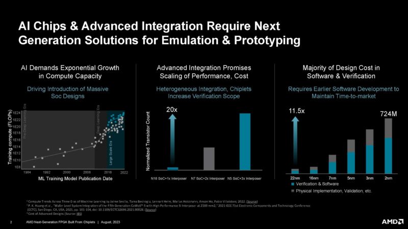
Since everything in 2023 is AI, even the tooling to build CPUs, GPUs, and AI accelerators, now have an AI spin.
![AMD XCVP1902 Next Gen Chiplet FPGA HC35 _Page_02](https://www.servethehome.com/wp-content/uploads/2023/08/AMD-XCVP1902-Next-Gen-Chiplet-FPGA-HC35-_Page_02-800x450.jpg)
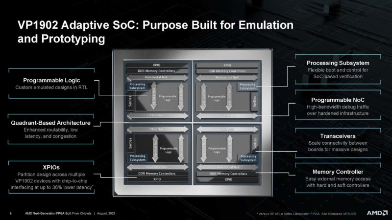
The VP1902 is deisgned not as much to be used as a single device, but instead to be used in more of a clustered fashion to help drive chip-scale verification and testing.
![AMD XCVP1902 Next Gen Chiplet FPGA HC35 _Page_03](https://www.servethehome.com/wp-content/uploads/2023/08/AMD-XCVP1902-Next-Gen-Chiplet-FPGA-HC35-_Page_03-800x450.jpg)
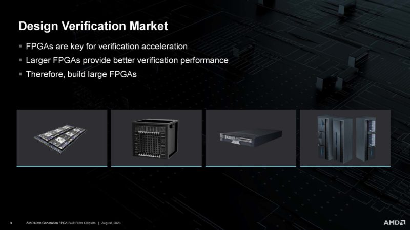
Here, big is good since FPGAs are not as dense as the chips they are prototyping. Bigger chips means either fewer FPGAs to hold all of the logic of a larger design or simply being able to fit larger designs into a cluster of these FPGAs.
![AMD XCVP1902 Next Gen Chiplet FPGA HC35 _Page_04](https://www.servethehome.com/wp-content/uploads/2023/08/AMD-XCVP1902-Next-Gen-Chiplet-FPGA-HC35-_Page_04-800x450.jpg)
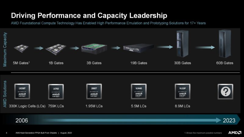
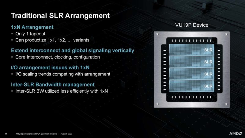
We saw the previous-gen VU19P at a winery after Hot Chips in 2019. You can see and learn about that here. Xilinx Virtex UltraScale Plus VU19P is a Big FPGA.
![AMD XCVP1902 Next Gen Chiplet FPGA HC35 _Page_05](https://www.servethehome.com/wp-content/uploads/2023/08/AMD-XCVP1902-Next-Gen-Chiplet-FPGA-HC35-_Page_05-800x450.jpg)
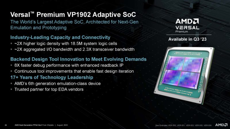
This is an AMD Versal Premium VP1902 adaptive SoC that is designed to be massive in scale.
![AMD XCVP1902 Next Gen Chiplet FPGA HC35 _Page_06](https://www.servethehome.com/wp-content/uploads/2023/08/AMD-XCVP1902-Next-Gen-Chiplet-FPGA-HC35-_Page_06-800x450.jpg)
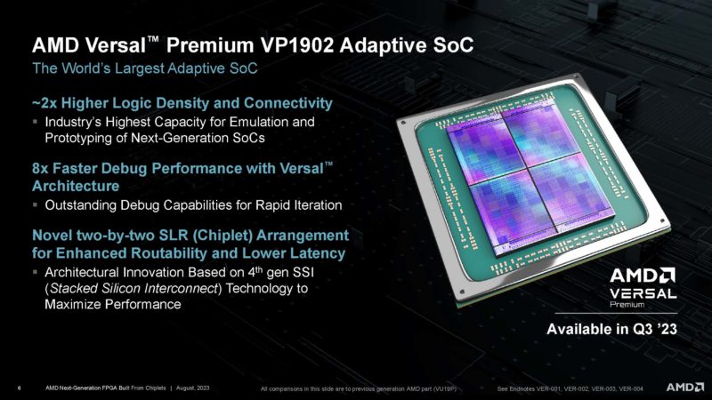
Using a 2×2 chiplet arrangement, along with generational enhancements, the VP1902 is able to roughly double the previous generation.
![AMD XCVP1902 Next Gen Chiplet FPGA HC35 _Page_07](https://www.servethehome.com/wp-content/uploads/2023/08/AMD-XCVP1902-Next-Gen-Chiplet-FPGA-HC35-_Page_07-800x450.jpg)
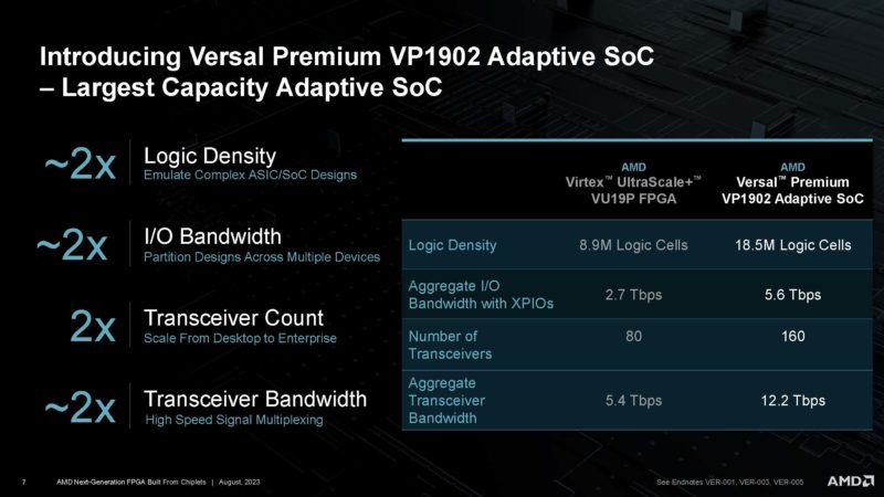
We went into the VP1902 in the previous piece, but here is a nice slide going over some of the highlights of the chip.
![AMD XCVP1902 Next Gen Chiplet FPGA HC35 _Page_08](https://www.servethehome.com/wp-content/uploads/2023/08/AMD-XCVP1902-Next-Gen-Chiplet-FPGA-HC35-_Page_08-800x450.jpg)
AMD is now talking about scaling up designs and using chiplets.
![AMD XCVP1902 Next Gen Chiplet FPGA HC35 _Page_09](https://www.servethehome.com/wp-content/uploads/2023/08/AMD-XCVP1902-Next-Gen-Chiplet-FPGA-HC35-_Page_09-800x450.jpg)
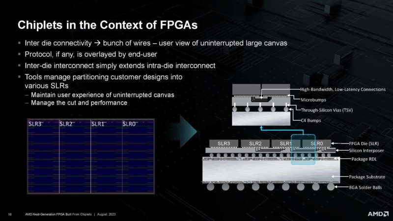
This is the inter-die connectivity and how the chip is packaged. FPGAs need to not just have chiplet-to-chiplet connectivity, but they often need to support extremely high-speed and dense external I/O.
![AMD XCVP1902 Next Gen Chiplet FPGA HC35 _Page_10](https://www.servethehome.com/wp-content/uploads/2023/08/AMD-XCVP1902-Next-Gen-Chiplet-FPGA-HC35-_Page_10-800x450.jpg)
Here is the chiplet in the previous VU19P.
![AMD XCVP1902 Next Gen Chiplet FPGA HC35 _Page_11](https://www.servethehome.com/wp-content/uploads/2023/08/AMD-XCVP1902-Next-Gen-Chiplet-FPGA-HC35-_Page_11-800x450.jpg)
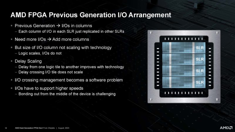
That approach had I/O columns that did not scale. What is really interesting here is that these long and wide chiplets are what Intel is showing with its Changing its Xeon CPU Architecture at Hot Chips 2023. A key difference is that the end cap dies are I/O for things like UPI, PCIe Gen5, and CXL in the Intel designs.
![AMD XCVP1902 Next Gen Chiplet FPGA HC35 _Page_12](https://www.servethehome.com/wp-content/uploads/2023/08/AMD-XCVP1902-Next-Gen-Chiplet-FPGA-HC35-_Page_12-800x450.jpg)
Here is how the quadrant approach, more similar to the current Sapphire Rapids Xeons is built. Stay tuned to the STH YouTube as our Intel Xeon Max video is almost ready to upload along with the accompanying article.
![AMD XCVP1902 Next Gen Chiplet FPGA HC35 _Page_13](https://www.servethehome.com/wp-content/uploads/2023/08/AMD-XCVP1902-Next-Gen-Chiplet-FPGA-HC35-_Page_13-800x450.jpg)
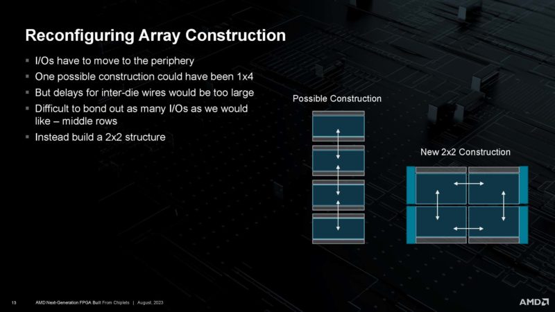
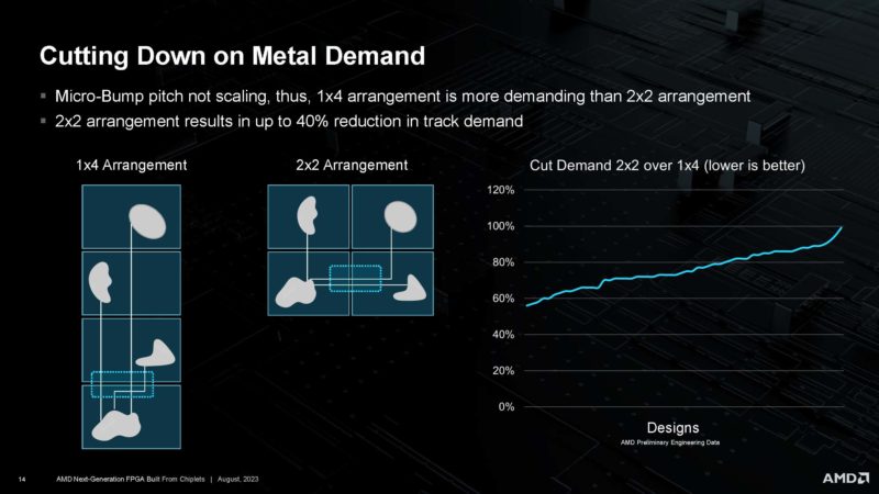
As part of this AMD is showing how using 2×2 over 1×4 leads to lower track demands.
![AMD XCVP1902 Next Gen Chiplet FPGA HC35 _Page_14](https://www.servethehome.com/wp-content/uploads/2023/08/AMD-XCVP1902-Next-Gen-Chiplet-FPGA-HC35-_Page_14-800x450.jpg)
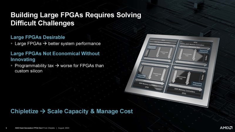
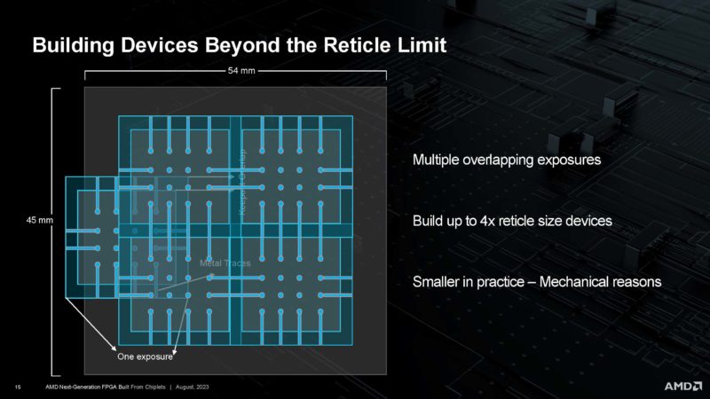
Chiplets also allow AMD to exceed the reticle limit for how big a monolithic chip (sans Cerebras) can be made.
![AMD XCVP1902 Next Gen Chiplet FPGA HC35 _Page_15](https://www.servethehome.com/wp-content/uploads/2023/08/AMD-XCVP1902-Next-Gen-Chiplet-FPGA-HC35-_Page_15-800x450.jpg)
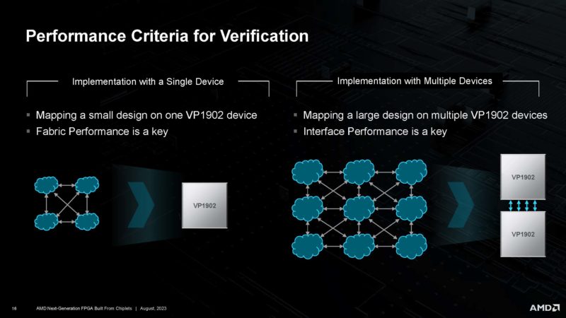
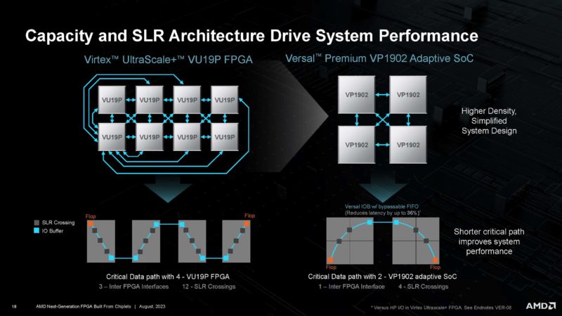
Now AMD is talking about performance criteria scaling to more devices.
![AMD XCVP1902 Next Gen Chiplet FPGA HC35 _Page_16](https://www.servethehome.com/wp-content/uploads/2023/08/AMD-XCVP1902-Next-Gen-Chiplet-FPGA-HC35-_Page_16-800x450.jpg)
Here is AMD’s performance metrics.
![AMD XCVP1902 Next Gen Chiplet FPGA HC35 _Page_17](https://www.servethehome.com/wp-content/uploads/2023/08/AMD-XCVP1902-Next-Gen-Chiplet-FPGA-HC35-_Page_17-800x450.jpg)
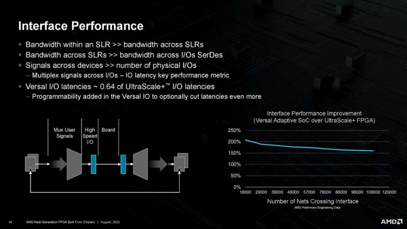
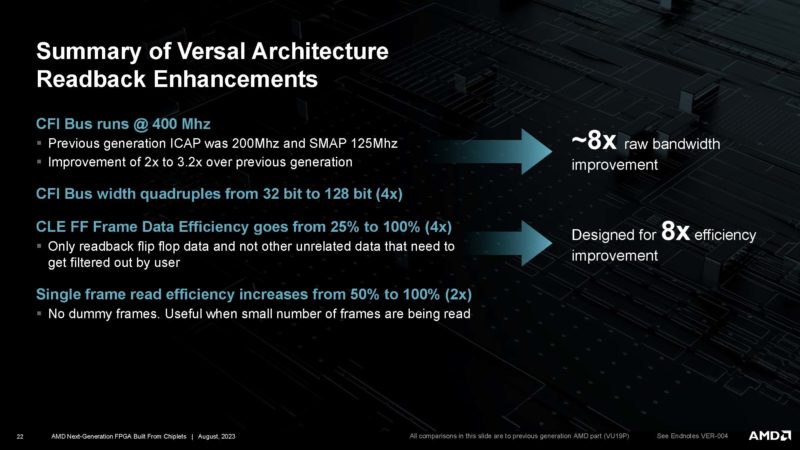
Here is more about the impact.
![AMD XCVP1902 Next Gen Chiplet FPGA HC35 _Page_18](https://www.servethehome.com/wp-content/uploads/2023/08/AMD-XCVP1902-Next-Gen-Chiplet-FPGA-HC35-_Page_18-800x450.jpg)
Here is the new interface performance:
![AMD XCVP1902 Next Gen Chiplet FPGA HC35 _Page_19](https://www.servethehome.com/wp-content/uploads/2023/08/AMD-XCVP1902-Next-Gen-Chiplet-FPGA-HC35-_Page_19-800x450.jpg)
ANd the readback performance for the FPGA fabric in verification.
![AMD XCVP1902 Next Gen Chiplet FPGA HC35 _Page_20](https://www.servethehome.com/wp-content/uploads/2023/08/AMD-XCVP1902-Next-Gen-Chiplet-FPGA-HC35-_Page_20-800x450.jpg)
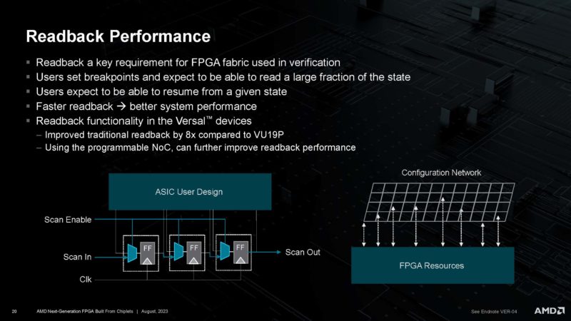
The new ability to get visibility into each register is a big deal for chip verification engineers.
![AMD XCVP1902 Next Gen Chiplet FPGA HC35 _Page_21](https://www.servethehome.com/wp-content/uploads/2023/08/AMD-XCVP1902-Next-Gen-Chiplet-FPGA-HC35-_Page_21-800x450.jpg)
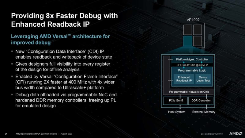
Here is a summary of what was just presented.
![AMD XCVP1902 Next Gen Chiplet FPGA HC35 _Page_22](https://www.servethehome.com/wp-content/uploads/2023/08/AMD-XCVP1902-Next-Gen-Chiplet-FPGA-HC35-_Page_22-800x450.jpg)
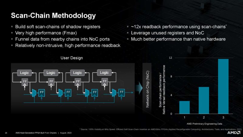
Here is AMD’s slide on the Scan-Chain Methodology.
![AMD XCVP1902 Next Gen Chiplet FPGA HC35 _Page_23](https://www.servethehome.com/wp-content/uploads/2023/08/AMD-XCVP1902-Next-Gen-Chiplet-FPGA-HC35-_Page_23-800x450.jpg)
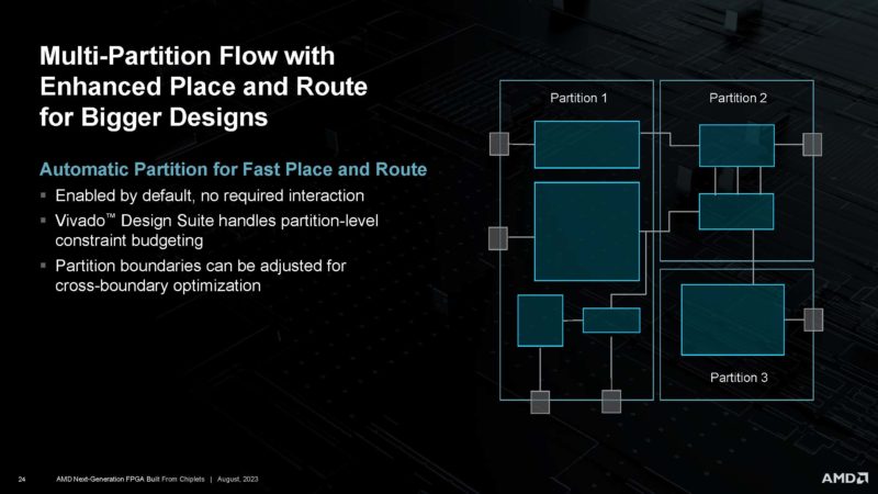
Here is AMD’s multi-partition flow for faster place and routing.
![AMD XCVP1902 Next Gen Chiplet FPGA HC35 _Page_24](https://www.servethehome.com/wp-content/uploads/2023/08/AMD-XCVP1902-Next-Gen-Chiplet-FPGA-HC35-_Page_24-800x450.jpg)
Here is the summary slide for the talk.
![AMD XCVP1902 Next Gen Chiplet FPGA HC35 _Page_25](https://www.servethehome.com/wp-content/uploads/2023/08/AMD-XCVP1902-Next-Gen-Chiplet-FPGA-HC35-_Page_25-800x450.jpg)
We just went through 25 slides in 30 minutes!
Final Words
Talk about reading the room! This was just about the perfect presentation to give at Hot Chips. AMD had a 30-minute detailed advertisement for its big chip design verification FPGA, to folks that design chips for a living.
We will probably never get to use one of these, but it is always cool to see the chips that make chips and just big new designs in general.