
Today, AMD has a new giant FPGA. The AMD VP1902 is set to be the world’s largest FPGA. Designed to offer a huge programmable logic array, this is the class of FPGA designed specifically to emulate future silicon designs of chips ranging from small SoCs found in Raspberry Pi’s to large next-gen accelerators like the AMD Instinct MI300. The previous generation Xilinx VU19P was the largest FPGA when it was launched, but the new VP1902 adds Versal features and adopts a new AMD chiplet design to more than double the key capabilities of the FPGAs.
AMD VP1902 is Leviathan FPGA Doubling the Previous-Gen Largest FPGA
Xilinx, now AMD has had a line specifically designed to help in the emulation and debugging of silicon for many years. For those that do not know, a very common approach to designing a chip is to use a tool to put the logic onto a series of large FPGAs and then emulate a design well before it goes to silicon manufacturing. As chips get larger, the number of gates that need to be used increases. There is not a real gate-to-transistor ratio, but folks have told us that 4 transistors in silicon roughly equate to 1 gate on these FPGAs is a reasonable approximation (with a LOT of variabilities.)
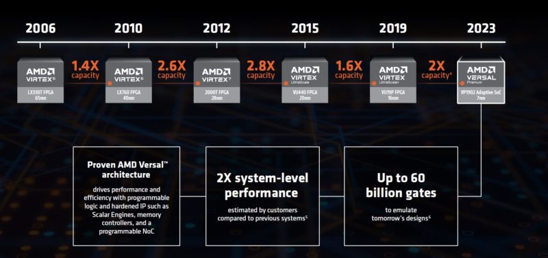
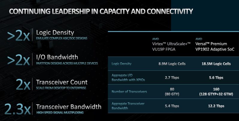
The new AMD Versal Premium VP1902 effectively doubles the gate count one can emulate with up to 18.5M logic cells. Along with the additional logic, AMD is adding more transceivers and more bandwidth on the transceivers to help connect more devices for a larger emulation capability. For some frame of reference, these scale from one or a few devices up to over 1000 connected FPGAs to emulate large silicon designs.
Beyond having more programmable logic cells, AMD also has a number of features as part of both its Versal Premium line, but also unique for this product. The new unique features compared to the AMD Xilinx VU19P are:
- New Processing System
- Programmable Network on Chip (NoC)
- Hardened DDR Memory Controllers (14x)
- Four 600G Ethernet MACs (Supports 100-400G Ethernet, 600G total BW)
- Twelve 100G Ethernet MACs (Supports 10-100G Ethernet)
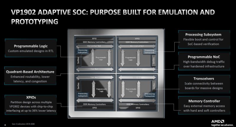
The new VP1902 has 16x PCIe Gen5 x4 hard IP blocks versus the VU19P which had 8x PCIe Gen4 x8. The HPIO to XPIO upgrade should result in a 36% lower latency scaling from chip to chip. There is even a big clock speed update. These new upgrades are significant, beyond just having more programmable logic cells.
All of that additional IP means that fewer programmable logic cells need to be used for this IP and so more of the floorplan can be used for emulation. AMD also has the capability to use its NoC for debugging and things like restoring designs to specific register states to help aid in the debugging process. This is without having to build all of this functionality as well.
Final Words
This is a huge chip, and AMD is doing something interesting. It has two sets of mirrored and rotated dies (four total) that are combined into a single package. If you just looked at this, you might first think it is a 4th Gen Intel Xeon Scalable Sapphire Rapids instead of an AMD design. Instead, it is the VP1902.
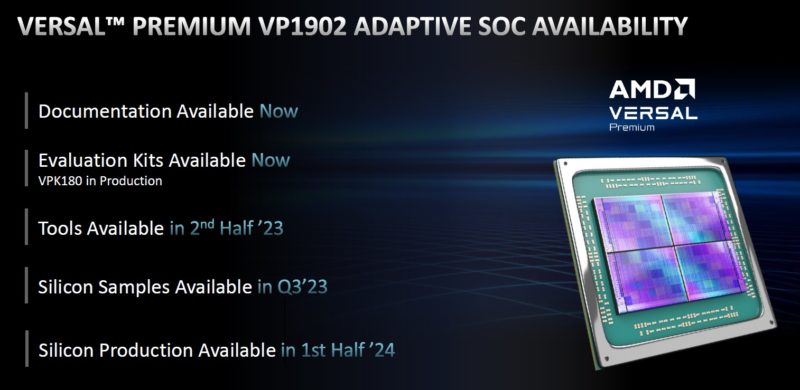
One of the coolest parts about AMD’s release is that silicon is coming soon with samples next quarter. Xilinx had a history of announcing silicon well before there was any glimmer of availability, so this is a welcome change.


The two sets of rotated dies is exactly how Sapphire Rapids is configured for the XCC products. nVidia’s old white paper on how to do MCM GPU followed a similar pattern. This schema seems to be relatively common in terms of how to do MCM packing like this. The odd ball was the older VU19P which added dies in a single dimension but conceptually could scale further as the middle dies were the same with the two at the ends being different designs (transceivers and some hard logic).
What is odd is that AMD didn’t announce this part alongside their big data center event a few weeks back. Granted FPGAs like this can be used a development tool but companies like Microsoft have leveraged FPGAs in their datacenters as a programmable accelerator. In fact, Microsoft was a big pusher of the Xeon + Altera FPGA combo package. I’m honestly surprised we haven’t seen an AMD Epyc + Xilinx FPGA combo product yet.
It sounds like a cool idea, but then where is the Xeon + Altera FPGA combo package that we can get ahold of? Seems like Intel has had a lot longer to work on that combo product than AMD. The Xilinx Alveo cards can be plugged into AMD or Intel servers to fill them up with different flavors of accelerator cards to more closely match your end app need:
https://www.xilinx.com/products/boards-and-kits/alveo.html
That seems like a better strategy than to make one single x86+FPGA chip. No matter how many resources are available on that combo chip, it is bound to not make everyone happy.
That VP1902 is a monster chip, but maybe someday there will be an accelerator card for it. I remember playing with a Virtex-5 LX330T device back in 2009. Took 8-hours for an Intel Core 2 Duo to build a simple design for it with ISE!
Doubling AMD/Xilinx’s largest FPGA…
Stratix 10 has more LE than this FPGA – and was multi die as well.
@Truth Teller
No, the largest Stratix 10 is the GX 10M with 10 million logic elements. Not even close to this one.
Logic Elementsts (Intel) and Logic Cells (AMD) are pretty similar but not exactly the same. Better comaprison is 3.5m 6-LUT for Stratix vs. 8.5 6-LUT for Versal (also not 100% the same).
@Kevin G
This won’t make a good accelerator because this is optimized for maximum number of logic and maximum memory (blockRAM, ultraRAM). This is not the Xilinx FPGA with the most multiplier units, That would be the VP2802 with more than twice the “DSP units”. The VP1902 is optimized for logic simulation and might end up as the gold-standard for this application in almost every company designing leading edge chips (Intel might refuse to buy).
Stratix 10 GX … 43.3 Billion transistors. on 14nm.
Intel is now offering CXL 2.0 hardened tiles on the Agilex 7, which should be a popular feature.
@JayN
Those are transistors of the chip, not transistors you can program your logic with. Nobody cares how many transistors the chip has.
The postings under this article here are absurd. They don’t seem to know what FPGAs are.
@Lasertoe
And people wonder why LLMs like ChatGPT constantly make things up. They’re trained on billions of similarly ignorant comments!
Comments are closed.