AMD EPYC 9004 Genoa Platform
AMD breaks its chip delivery into two parts, the SoC, and then the platform enabled by the SoC. Here is the key overview slide. We have already discussed the top left side with the Zen 4 changes. So let us now get to the rest of the chip.
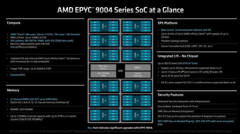
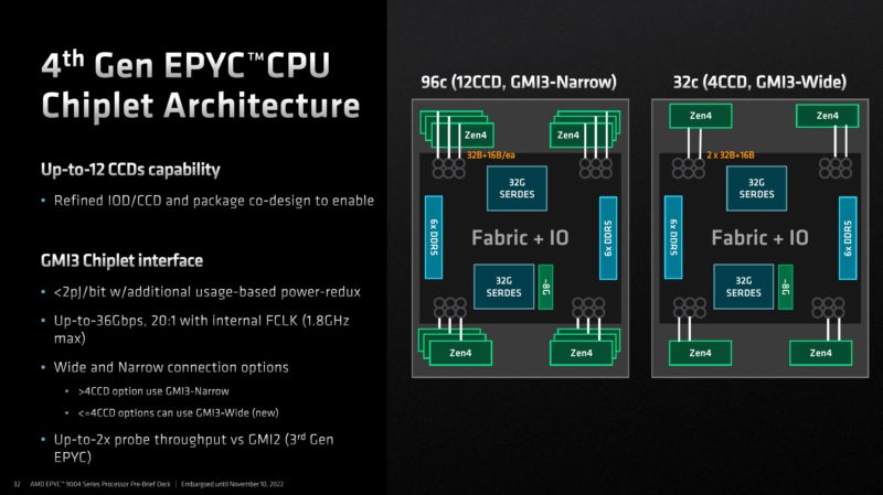
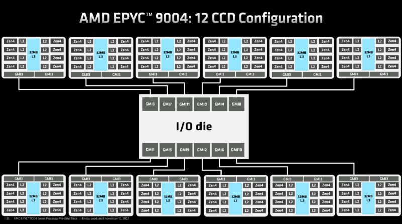
The 4th Gen EPYC CPU scales in the number of (up to) 8 core CCDs from 4 to 12. The halo part at 96 cores (and the 84-core variant) will utilize 12 CCDs. Lower core count options can use fewer CCDs. Such as 8 or 4. The 4x CCD variants (up to 32 cores) have an interesting trick where they can get 2x the links to the IO die per CCD. The 12 and 8 CCD variants only have one GMI3 link to the IO die.
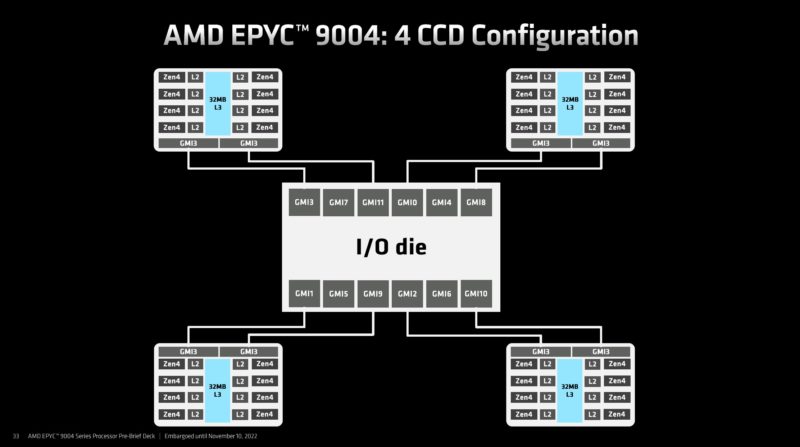
Here is a look at that 4x CCD configuration with two GMI3 links to the IOD per CCD.
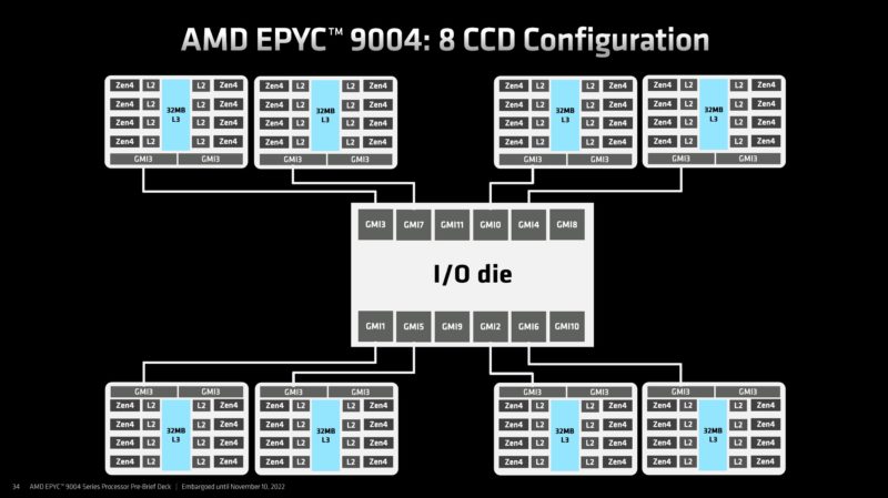
Here is the 8 CCD version of that where each CCD gets a single GMI3 connection
On the 12 CCD chips, all CCDs have a single GMI3 link to the IO die.
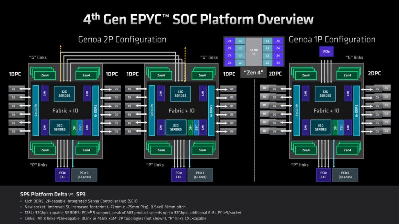
That is how the CCDs and IO die are connected, but then comes building out the rest of the system with I/O and memory. That is what gives us single and dual-socket servers.
AMD has a new generation of its Infinity Fabric interface which is AMD’s socket-to-socket interconnect. Infinity Fabric gets another speed bump in this generation. AMD’s Infinity Fabric uses SerDes that also can handle things like PCIe and so as those SerDes get faster for PCIe, Infinity Fabric follows suit. AMD moving from PCIe Gen3 era to Gen5 era on the links means that the interconnect bandwidth is now massive.
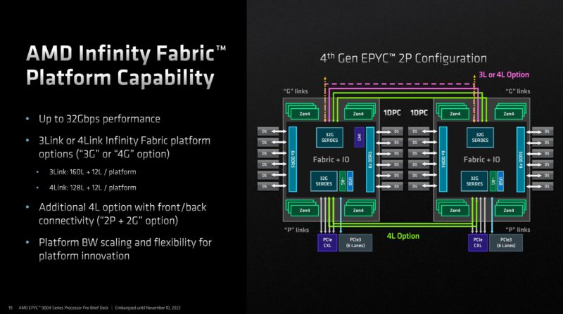
In the above diagram, you may notice that there are 3Link and 4Link options. AMD now has so much interconnect bandwidth that some customers will decide that three links are enough. The fourth link that requires an x16 port on the other end can be configured to instead operate as PCIe Gen5 x16 on each CPU, giving us 160x PCIe Gen5 lane configurations in 2P servers. We first covered this in Dell and AMD Showcase Future of Servers 160 PCIe Lane Design. Many applications such as storage and GPU servers were already finding that with the previous PCIe Gen4 era of Infinity Fabric only three socket-to-socket links were needed instead of four. Here is what this functionality can look like in a dual-socket server:
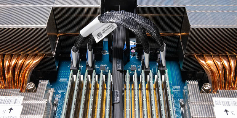
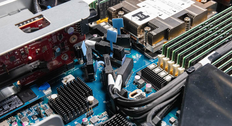
The cabled connections are part of the socket-to-socket interconnect. Not only does that free up some motherboard trace requirements, but it also allows the same connectors to be used for PCIe instead by simply using different (longer) cables connecting to PCIe devices. In this server, these links are forward of the CPUs making them closer to the front panel for servicing PCIe Gen5 SSDs and accelerators. In the above example, these are configured socket-to-socket, but the other option is that they can be re-routed to other components such as front panel NVMe SSDs or even FPGAs, AI accelerators, or GPUs.
This functionality is due to the awesome SerDes that EPYC employs, and has employed for generations. Each CPU has 128 lanes that are generally broken up into x16 segments. 64 (or 4×16) are xGMI (socket-to-socket Infinity Fabric) and PCIe Gen5 capable. The other 64 lanes are xGMI, PCIe, CXL, and SATA capable. SATA is so slow compared to PCIe Gen5 x1 lanes that it is a very inefficient use of lanes. AMD still supports it, but at some point, we expect support to be dropped and a small amount of transistor count to be reclaimed. Those same 64 (4x 16) can also be used for CXL.
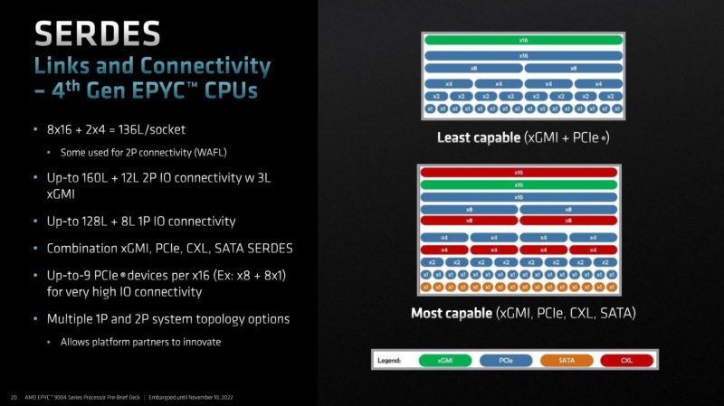
You may also notice on the slide above a few features. First, one can have up to 9 devices on a x16 root but the bifurcation can go down to x1. The other big one is the IO connectivity lanes. These are PCIe Gen3 lanes, not Gen5. AMD has a few extra lanes for things like motherboard low-speed SATA connections, 1/10GbE NICs, and so forth instead of a single WAFL lane (WAFL still lives in Genoa.) In dual-socket servers, one gets 12 extra lanes, and in a single socket 8 extra lanes. The difference is that two of the eight in each CPU are used for inter-socket communication in dual-socket configurations.
The impact of this is that AMD is able to get 128 PCIe Gen5 lanes (up to 64x can be CXL) in a single socket plus eight PCIe Gen3 lanes for miscellaneous functions. It would be strange to say that is a 136 PCIe lane CPU because of the vastly different speeds, but that is one way to look at it. In dual socket configurations, we will see 2x 64 = 128 or 2x 80 = 160 PCIe Gen5 lanes depending on the socket-to-socket xGMI link configuration mentioned earlier. Add another 12 PCIe Gen3 lanes and we get up to 172 total lanes, but only up to 160 PCIe Gen5 lanes.
Gen 5 is going to add a lot of cost to systems. OEMs have told us that the signaling challenges are becoming formidable. Cabled connections cost more, but can bridge further distances. Even with cabled connections, we are seeing views like this where connectors are angled to help with bend radius and shorter cabled runs. PCIe Gen5 is fast, but it also adds cost to systems.
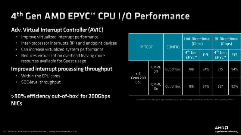
AMD also has a new AVIC controller. This helps with interrupt performance and means that out of the box, the new chips can almost saturate 200Gbps links. With 100Gbps, AMD platforms could saturate the links, but there were more configuration steps to get that to work.
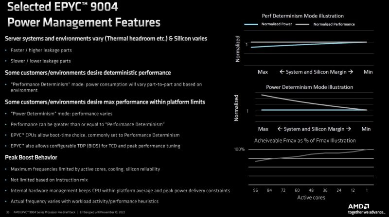
AMD also has new power management features. Something that many do not know you can do on AMD platforms is set performance or power-focused profiles. In performance determinism mode, performance is maintained across all chips. This is standard and what you see most benchmarks on. In power determinism mode, one gets to play the “silicon lottery” a bit and set a power level and let the EPYC chips in a system run at whatever performance level they can achieve. We did not get to play with this as much as we wanted but in about 30 minutes running a few workloads we were able to eke out about 2% better performance but also with a bit higher overall power consumption (~50W) using power determinism. That is not going to make the main piece because we did not have time to really profile that result, but it seemed to be clearly doing something.
Next, let us get to the memory and CXL 1.1 implementation.


Any chance of letting us know what the idle power consumption is?
$131 for the cheapest DDR5 DIMM (16GB) from Supermicro’s online store
That’s $3,144 just for memory in a basic two-socket server with all DIMMs populated.
Combined with the huge jump in pricing, I get the feeling that this generation is going to eat us alive if we’re not getting those sweet hyperscaler discounts.
I like that the inter CPU PCIe5 links can be user configured, retargeted at peripherals instead. Takes flexibility to a new level.
Hmm… Looks like Intel’s about to get forked again by the AMD monster. AMD’s been killing it ever since Zen 1. So cool to see the fierce competitive dynamic between these two companies. So Intel, YOU have a choice to make. Better choose wisely. I’m betting they already have their decisions made. :-)
2 hrs later I’ve finished. These look amazing. Great work explaining STH
Do we know whether Sienna will effectively eliminate the niche for threadripper parts; or are they sufficiently distinct in some ways as to remain as separate lines?
In a similar vein, has there been any talk(whether from AMD or system vendors) about doing ryzen designs with ECC that’s actually a feature rather than just not-explicitly-disabled to answer some of the smaller xeons and server-flavored atom derivatives?
This generation of epyc looks properly mean; but not exactly ready to chase xeon-d or the atom-derivatives down to their respective size and price.
I look at the 360W TDP and think “TDPs are up so much.” Then I realize that divided over 96 cores that’s only 3.75W per core. And then my mind is blown when I think that servers of the mid 2000s had single core processors that used 130-150W for that single core.
Why is the “Sienna” product stack even designed for 2P configurations?
It seems like the lower-end market would be better served by “Sienna” being 1P only, and anything that would have been served by a 2P “Sienna” system instead use a 1P “Genoa” system.
Dunno, AMD has the tech, why not support single and dual sockets? With single and dual socket Sienna you should be able to be price *AND* price/perf compared to the Intel 8 channel memory boards for uses that aren’t memory bandwidth intensive. For those looking for max performance and bandwidth/core AMD will beat Intel with the 12 channel (actually 24 channel x 32 bit) Epyc. So basically Intel will be sandwiched by the cheaper 6 channel from below and the more expensive 12 channel from above.
With PCIe 5 support apparently being so expensive on the board level, wouldn’t it be possible to only support PCIe 4 (or even 3) on some boards to save costs?
All other benchmarks is amazing but I see molecular dynamics test in other website and Huston we have a problem! Why?
Olaf Nov 11 I think that’s why they’ll just keep selling Milan
@Chris S
Siena is a 1p only platform.
Looks great for anyone that can use all that capacity, but for those of us with more modest infrastructure needs there seems to be a bit of a gap developing where you are paying a large proportion of the cost of a server platform to support all those PCIE 5 lanes and DDR5 chips that you simply don’t need.
Flip side to this is that Ryzen platforms don’t give enough PCIE capacity (and questions about the ECC support), and Intel W680 platforms seem almost impossible to actually get hold of.
Hopefully Milan systems will be around for a good while yet.
You are jumping around WAY too much.
How about stating how many levels there are in CPUS. But keep it at 5 or less “levels” of CPU and then compare them side by side without jumping around all over the place. It’s like you’ve had five cups of coffee too many.
You obviously know what you are talking about. But I want to focus on specific types of chips because I’m not interesting in all of them. So if you broke it down in levels and I could skip to the level I’m interested in with how AMD is vs Intel then things would be a lot more interesting.
You could have sections where you say that they are the same no matter what or how they are different. But be consistent from section to section where you start off with the lowest level of CPUs and go up from there to the top.
There may have been a hint on pages 3-4 but I’m missing what those 2000 extra pins do, 50% more memory channels, CXL, PCIe lanes (already 160 on previous generation), and …
Does anyone know of any benchmarking for the 9174F?
On your EPYC 9004 series SKU comparison the 24 cores 9224 is listed with 64MB of L3.
As a chiplet has a maximum of 8 cores one need a minimum of 3 chiplets to get 24 cores.
So unless AMD disable part of the L3 cache of those chiplets a minimum of 96 MB of L3 should be shown.
I will venture the 9224 is a 4 chiplets sku with 6 cores per chiplet which should give a total of 128MB of L3.
EricT – I just looked up the spec, it says 64MB https://www.amd.com/en/products/cpu/amd-epyc-9224
Patrick, I know, but it must be a clerical error, or they have decided to reduce the 4 chiplets L3 to 16MB which I very much doubt.
3 chiplets are not an option either as 64 is not divisible by 3 ;-)
Maybe you can ask AMD what the real spec is, because 64MB seems weird?
@EricT I got to use one of these machines (9224) and it is indeed 4 chiplets, with 64MB L3 cache total. Evidently a result of parts binning and with a small bonus of some power saving.
Comments are closed.