
At SC21 we got additional details around Intel Sapphire Rapids, the next-generation Intel Xeon platform. We had the opportunity to chat with Intel prior to SC21 and have a bit more market context around the new chips. Intel also is highlighting the Aurora supercomputer at SC21.
Intel Sapphire Rapids Update at SC21
First, Intel has its Sapphire Rapids Xeon and the HBM model. We have covered these previously at STH. Above that in terms of capability and integration, there is Ponte Vecchio Intel’s high-end HPC GPU/ accelerator. As no surprise, Intel expects to continue making new chips.
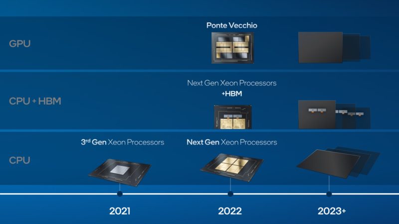
For 2022 though, the big ones are Sapphire Rapids for the Xeon side and Ponte Vecchio for the GPU.
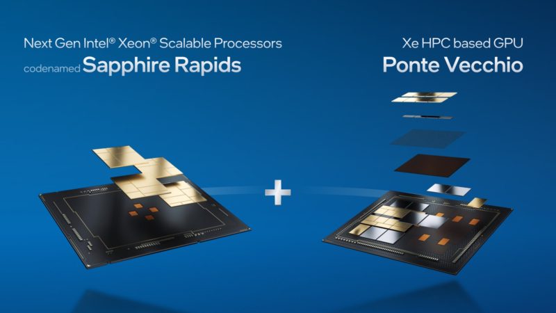
We have covered Intel Details Sapphire Rapids several times now. We even saw Samsung showing Intel Sapphire Rapids PCIe Gen5 Server at OCP Summit 2021 and a Flex Bodega Bay Intel Xeon Sapphire Rapids System.
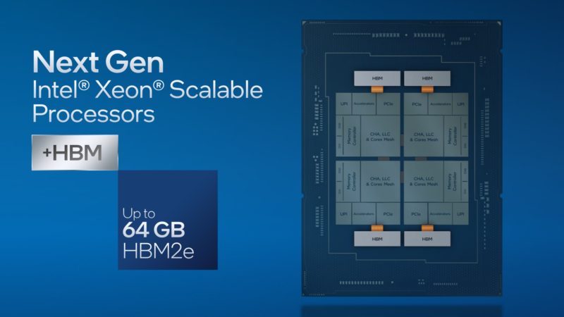
Perhaps the big new disclosure is that Intel is using 64GB of HBM2e on Sapphire Rapids. We just saw HBM3 last week in our Wild Hardware of OCP Summit 2021 Speed Run. Given the product timing we get HBM2e as we see on accelerators like the NVIDIA A100 80GB today.
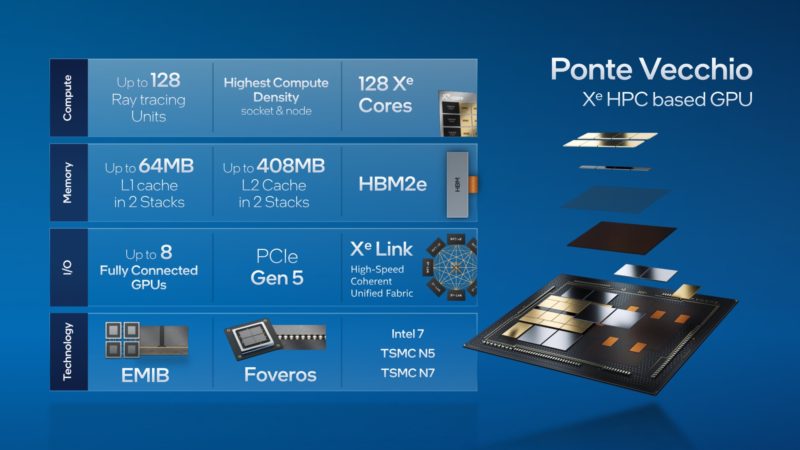
On the Ponte Vecchio side we get 408MB of L2 cache and lots of performance. Intel is productizing 4, 6, and 8 GPU configurations. This is similar to how NVIDIA is selling its Redstone and HGX A100 8x GPU platforms.
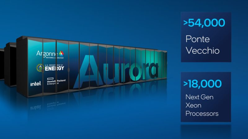
Intel also said that Aurora has over 54,000 Ponte Vecchio GPUs and 18,000 Sapphire Rapids processors. You will note this is a 6:1 ratio. That is something we knew about previously.
In the final words a quick recap of a few questions.
Final Words
Intel is releasing information about its new chips at an excruciatingly slow pace. Still, it is good to get new disclosures.
One of the big questions that I asked Jeff McVeigh VP and GM of HPC at Intel about was about HBM versus non-HBM Sapphire Rapids Xeon mix in the market. As one would expect, we did not give exact pricing, but he did indicate that the HBM2e equipped processors would carry a significant price premium. As such, it seems like Intel is expecting these to be very different segments. This is expected, but we have had some readers assume that Sapphire Rapids’s popular SKUs would be the HBM2e version. It seems like Intel is expecting higher volumes on the non-HBM models. That makes perfect sense, but it is also a good confirmation.
Another item I asked Jeff about was how to view Ponte Vecchio. I teed up the question noting that NVIDIA seems keen to position its data center accelerators as AI accelerators while the AMD Instinct MI200 seems to be focused on HPC. Jeff said that he expects Ponte Vecchio to target both workloads. Time will tell a bit on that one, but the other key on this question is that Jeff noted that he expected PV to be competitive in both realms. My sense is that Intel probably has some sense of what its competition is offering customers, so this may be a big opportunity for Ponte Vecchio.
Now, we just need to get to 2022 so we can see these chips in the wild since their platforms are already being shown off!


Regarding the competitiveness:
Basic math is already showing us that PVC at 54k+ GPUs @2EF+ is not really competitive with MI200 series for simple FP64 matrix multiplication (aka simple HPC FEM computation).
PVC would reach ~40TF matrix FP64, while MI200 reaches ~90TF matrix FP64.
We don’t know much about the PVC vector performance though. If it’s the same as matrix that would be on par with ~45 TF vector FP64 for MI200
PVC can also be interesting for “niche” applications where the big caches are useful.
+ By the time PVC comes to market we might even have new GPUs from NVIDIA/AMD as competitors.
“Basic math is already showing us that PVC at 54k+ GPUs @2EF+ is not really competitive with MI200 series for simple FP64 matrix multiplication (aka simple HPC FEM computation).
PVC would reach ~40TF matrix FP64, while MI200 reaches ~90TF matrix FP64.”
I believe you are making an assumption that Aurora’s 2 exaflops is referring to matrix arithmetic. The RPeak has always referred to vector arithmetic and I think it’s more likely that’s what they mean. So Ponte Veccho should have about 40 teraflops of FP64, which is close to the throughput of the MI200 accelerators. Besides, I could be wrong, but I don’t think Intel has talked about FP64 matrix operations for Ponte Vecchio. I see mention of TF32, FP16, BF16, and INT8 for the matrix engines. I think the FP64 matrix operation is an extremely niche operation at the moment.
“By the time PVC comes to market we might even have new GPUs from NVIDIA/AMD as competitors.”
Neither Ponte Vecchio nor MI200 will be used extensively outside supercomputers. Neither Intel nor AMD have the software stack for it. Intel might claim they are “targeting both [AI and HPC]” but they are unlikely to get much traction in AI with this first generation of GPUs (in fact they are unlikely to get much traction in HPC, either). NVIDIA will have new supercomputer hardware soon after Ponte Vecchio arrives, but since the MI200 is just coming out I doubt AMD will.
It looks like the big differences between the Ponte Vecchio and MI200 GPUs are cost and power usage. Since AMD has announced several other supercomputer wins and Intel has not, it’s a fair bet that AMD wins at those.
“As one would expect, we did not give exact pricing” Heh, I would think not, given that you were asking Intel for information on the chips, not the other way around! :D
From what I’ve seen in the leaks, Intel marketing sapphire rapids to the high end is not surprising given that the leaked roadmaps indicated that the mainstream server space will largely or perhaps even exclusively continue to see icelake chips as the offering from Intel for an extended period of time. HEDT though will supposedly be sapphire rapids, so I guess we will see what the market segmentation does to those chips if those launch.
@Matt
“I think the FP64 matrix operation is an extremely niche operation ”
FP64 matrix multiplications are by far the most important operations for “supercomputers” (With or without dedicated matrix units). That’s why LINPACK(and TOP500) is mostly FP64 matrix multiplication. A100 equipped supercomputers use the FP64 tensor cores.
Rpeak is based on the theorateical max for LINPACK, thus mostly matrix FP64 too.
Typical HPC applications like FEM or CFD are also just FP64 matrix multiplications.
BTW The MI100 was released november 2011, so a MI300 in 2022 might be possible (even though I expect a 23 launch for El Capitan).
I think I made a mistake in assuming the MI200 @ ~90TF for this comparison as they usually compute Rpeak at base clock, not boost clocks (ha always been the case for CPUs and when I look at A100 supercomputers in TOP500 it’s the same there too).
My guess now: ~40 TF (PVC) vs 60-70 TF ( MI250(x) ) FP64 for Rpeak comparison in TOP500 list.
Looking at the A100 peak numbers, it seems you are right that Linpack is using the matrix operations. How much those operations are used throughout the codebases, I’m skeptical. Are you sure they are using mostly matrix-matrix operations in FEM and CFD and are not making mostly matrix-vector calculations? If matrix operations were really so ubiquitous it wouldn’t have taken AI functionality to spur the addition of matrix engines to the accelerators. Regardless, you need to compare the MI200’s vector performance with Ponte Vecchio’s vector performance. Intel is promising 32,768 FP64 ops per clock in vector performance. That means if the GPU runs at 1.1 GHz it has 36 TFlops FP64. Aurora is supposed to have about 54,000 Ponte Vecchios with a total peak performance exceeding 2 exaflops. 2,000,000 / 54,000 is about equal to 37 TFLops per GPU. So unless Intel is running their Ponte Vecchio GPUs at about 600 MHz their peak performance calculations are based on their FP64 vector performance. Like I said, I’m skeptical how ubiquitous the matrix operations actually are in supercomputing, but regardless, you cannot accurately compare the throughput of two fundamentally different operations.
AMD announced the MI100 at the same time last year as the MI200 was announced this year. If we follow that “pattern” for the MI300 announcement, which seems to be your reasoning, it would be a year from now. Ponte Vecchio will be “out” before that.
> Intel also said that Aurora has over 54,000 Ponte Vecchio GPUs and 18,000 Sapphire Rapids processors. You will note this is a 6:1 ratio.
Isn’t this 3:1 not 6:1, or are we counting something else than processor counts?
It’s 3:1. I believe each node will have 6 Ponte Vecchio GPUs and 2 Sapphire Rapids CPUs, so that’s probably where the confusion came from that led to the typo.
Any additional info on the gen3 Optane? The only thing I’ve seen on it is that it would be compatible with the DDR5 controller on Sapphire Rapids. Did they also hit DDR5-4800 speeds, for example?
intel highlighting frontier…?? amd is grinning. i think you meant to say intel highlighting aurora.
Comments are closed.