
We are a bit behind getting this one out, make that very far behind. August turned into a rapid pace due to Architecture Day 2021 then Hot Chips, so we have a few pieces that we never got to. At some point, we still need this piece up to reference in the future, as Alder Lake arrives, so we wanted to get it up before that cycle hits.
Intel Gracemont Low Power x86 Cores
As a “mont” processor, we know this comes from the Intel Atom lineage. Let us be perfectly clear, today’s Atom processors are not as fast as the big x86 cores from Intel, but they are no longer the same very slow cores we saw in the Atom D525 days as they started migrating to low power severs. Today’s Atom cores are perfectly capable of running many workloads that would have required an Intel Xeon E5-2600 Sandy Bridge series processor in years past, just at dramatically lower power. With Gracemont, Intel needs something that is perhaps more akin to an Arm Neoverse N1 core. That is to say, something that can run many workloads at a smaller silicon footprint and at a lower power figure. For the desktop, these are the efficient offload cores for Intel in Alder lake.
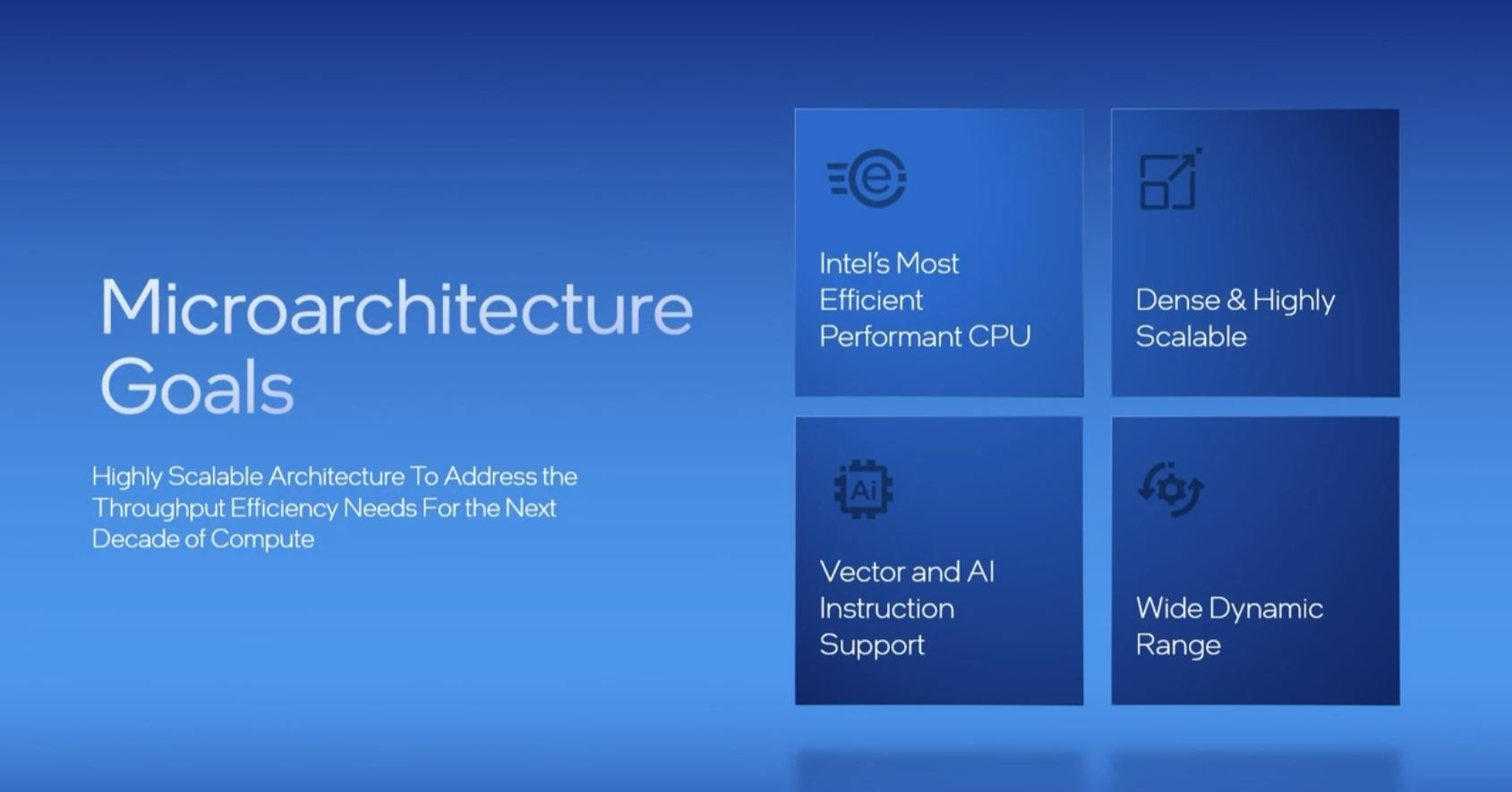
Key to doing that is building a core that is taking advantage of the areas where Intel can drive efficient compute, rather than trying to optimize for maximum performance.
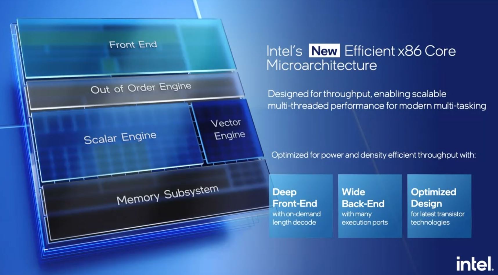
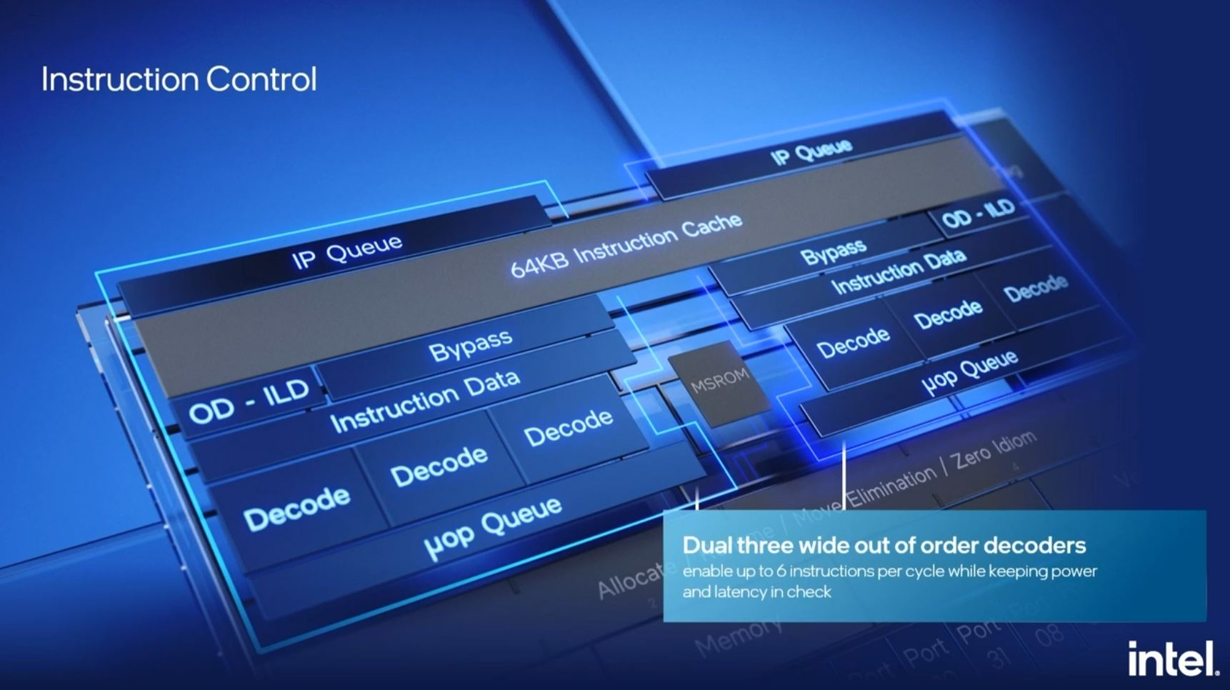
On the front-end, we still have the three wide out of order decode but we now have a 64KB L1 instruction cache, up from 32KB. Intel also has an on-demand decoding function that can handle up to six uops into the queues.
We also get a bigger branch target cache and prefetchers at all levels. Many modern designs focus on a key problem which is keeping execution units fed, and that is why we are seeing a lot of work on branch prediction here, but also as the broader industry rolls out new lines.

Intel also has increased the out of order window to 256 entries. It is fun to see how far the Atom line has come since being introduced as an in-order architecture thirteen years ago.
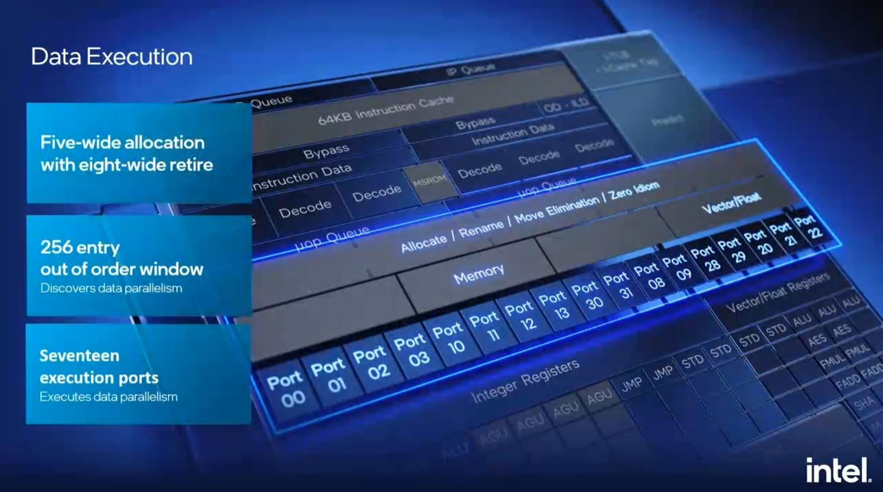
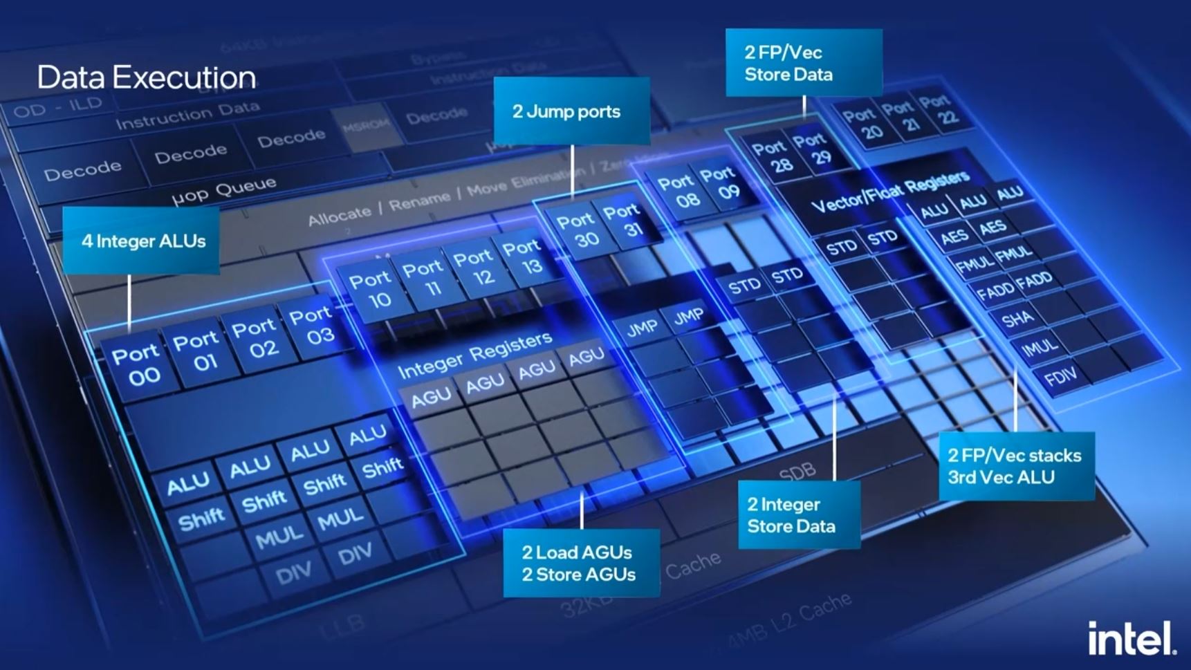
The data execution ports get a big upgrade here to a total of seventeen that are enumerated on the slide below. This is up from twelve on the previous generation.
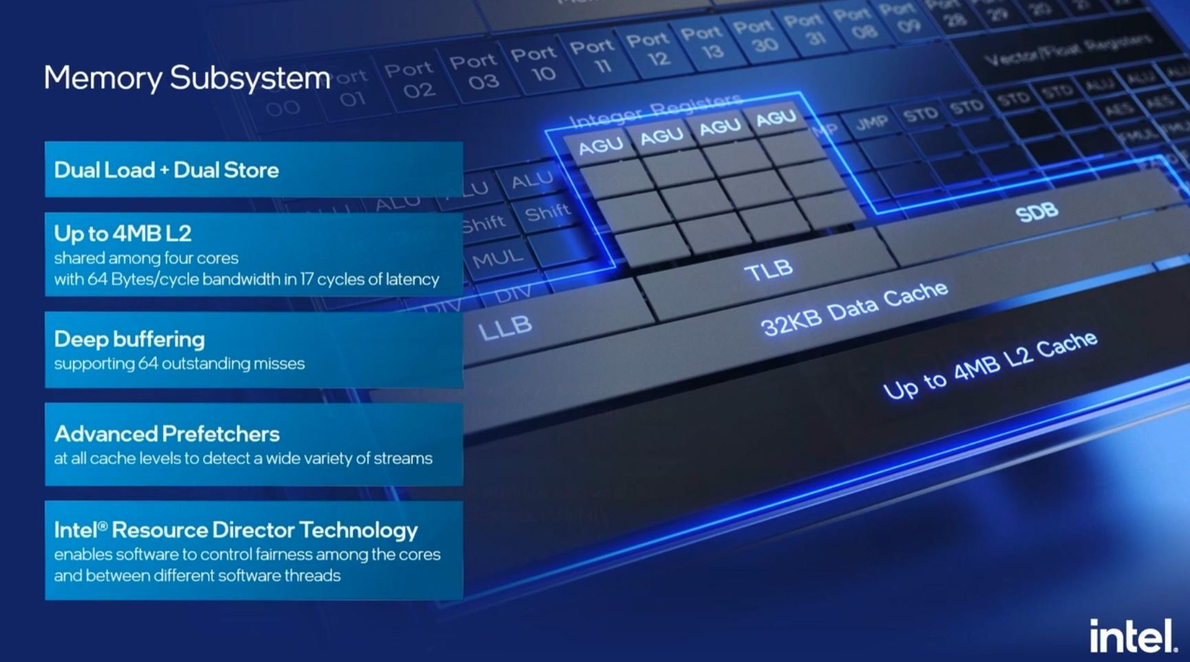
On the memory subsystem we get up to 4MB of L2 cache shared among four cores. Intel can vary caches based on SKU needs. Intel also has buffers and prefetchers to help efficiently use the caches.
Intel is adding AVX2 here and VNNI. We are going to see some base level of inference support on Intel’s products going forward. Intel’s direction here is basically that AI will be everywhere and therefore its processors should have a minimum amount of capability. Effectively by raising the bar of what the CPU can do, it removes many use cases where a dedicated accelerator is necessary. When industry benchmarks are run, like MLPerf Inference v1.1 the focus is on peak performance. Intel’s position is that its CPUs often run mixed workloads so it needs to account for inference acceleration as part of its offering, but not as the main focus.
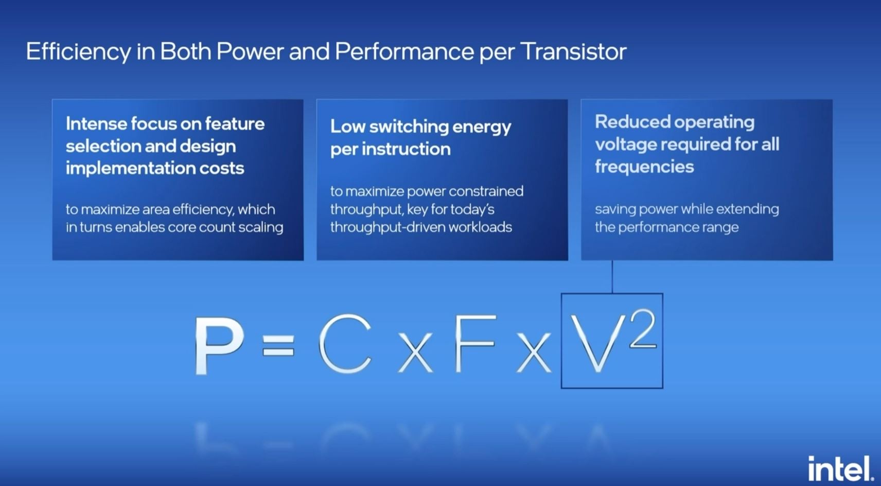
Something that is key here is that Intel is optimizing on low voltage and low power rather than maximum performance. That will also likely mean that we will see lower clock speeds than the larger cores, but that is also the point of the Atom line.
This is a huge jump in the Atom architecture.
Final Words
Intel threw out some figures such as the concept that four of its E-cores (this Gracemont core) can fit into about the same die area as its performance core (P-core) series like Skylake.
The big benefit is that it says it can deliver performance at lower power than Skylake but not necessarily the same maximum frequencies. In Alder Lake, these E-cores will be somewhat like offload cores that background tasks migrate to in order to free up the Intel Golden Cove Performance Cores (P-cores.) In the future, we can imagine where Intel may use these cores as alternatives when customers need higher core counts instead of maximum frequency or general-purpose performance per core. Golden Cove is important for Intel’s story positioning against AMD. Gracemont is important for Intel’s position against not just AMD but also Arm.


Fluff. Puff. Not trying to be mean, but that’s what this is.
“It is fun to see how far the Atom line has come…”
Seriously?
I’m actually surprised that Intel is not offering a high core count Xeon based around these cores as an alternative to Sapphire Rapids. There are plenty of workloads that scale well with core count that don’t inherently need the highest per thread performance. For example web servers and office virtual desktop environments fit such a profile. Clock speeds would be around where Sapphire Rapids would be in the data center already and with Sky Lake-like performance, these would be more than adequate for many additional use cases. If Intel can produce a 56-core Sapphire Rapids chip and these cores are about a quarter the side, producing a 64 core tile * 4 for a 256 core per package product seems feasible. That’s some good density before even scaling up the number of sockets.
Kevin G: excellent idea, but Snow Ridge “just” got release (err, year ago) and is based on Tremont uarch so we’ll need to wait a year or two to see Gracemont network atoms I guess. What a pity this would excellently compete with Ampere Altra I guess.
https://ark.intel.com/content/www/us/en/ark/products/codename/87586/products-formerly-snow-ridge.html
Thanks for this … best coverage I’ve seen on Gracemont architecture.
There were leaked slides on a Grand Ridge successor to Snow Ridge, using Gracemont cores, but perhaps a victim of the Intel-4 delay.
There have also been rumors of a Sierra Forest server chip in the works, maybe in 2023, which will be composed of a successor of Gracemont.
Comments are closed.