
Today at GTC 2021, we have a few major data center announcements from NVIDIA. Perhaps none are bigger than the NVIDIA Grace announcement. NVIDIA is signaling its full support for Arm with a new platform it is calling “Grace”. Effectively, NVIDIA is on the path to remove the need for an x86 CPU in certain scenarios.
NVIDIA Grace
Perhaps the biggest hardware announcement of GTC 2021 is that NVIDIA is finally getting into the server CPU business. As one may expect with a pending Arm acquisition, NVIDIA is planning to use off-the-shelf Arm cores to create a new CPU to align with its GPU.
NVIDIA was light on details (however we will go into more later) but the basic diagram of where Grace will fit can be shown below:
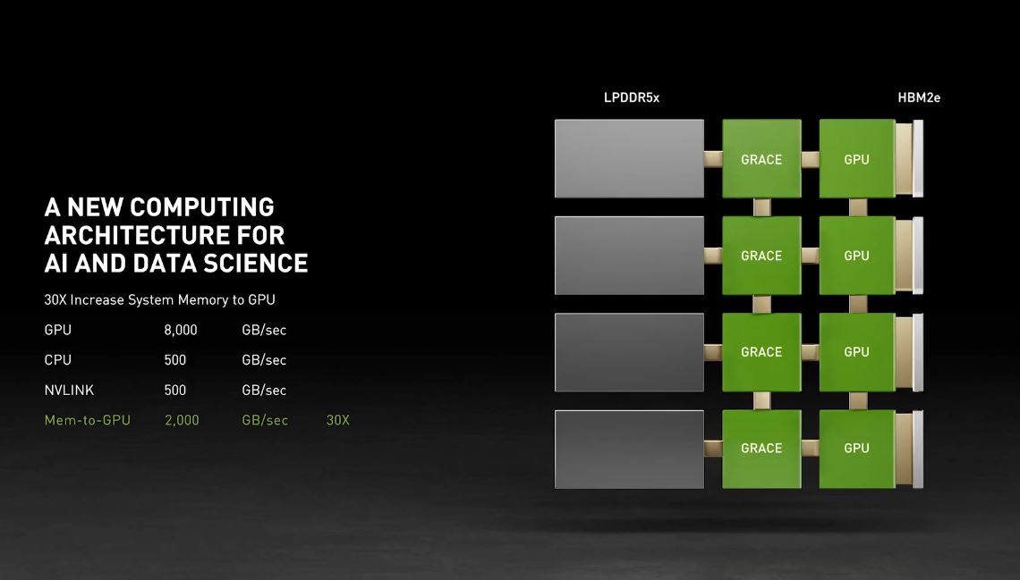
Effectively, NVIDIA has an Arm CPU core complex tied with next-gen NVLink support. It also is using LPDDR5x to controllers on the CPU to deliver higher memory bandwidth. Effectively, it is taking the general-purpose CPU, and hanging fast memory, and interconnect to GPUs off of each. This is largely about increasing memory bandwidth that we will discuss a bit below.
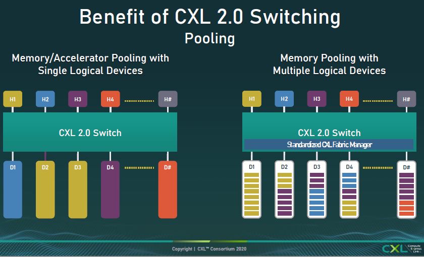
One of the other aspects of this announcement is related to context. In 2023, as Grace arrives, we will start seeing CXL 2.0. CXL 2.0 is a big deal. This is where we get switching and pooling. Effectively the way some vendors are looking at the memory bandwidth/ CPU bottleneck problem is not adding Arm CPUs in a 1:1 ratio. Instead, it is to take advantage of the high-performance and industry-standard CXL environment. With the Grace model, GPUs will have to go to the CPU to access memory. In the CXL 2.0 model, GPUs can directly share memory reducing the need for data movement and copies.
While we are excited by CXL 1.x in 2022 CPUs, 2023 is when the big architectural shifts will happen. Grace represents NVIDIA doing something different which makes it interesting. It also needs to show how/ why it is using Arm cores. While it may be partnering with Ampere and Altra today, it is hard to imagine how Ampere’s Arm platform for CUDA is relevant in the NVIDIA Grace era unless it leans into CXL heavily.
NVIDIA Grace: A Warning Shot to Partners
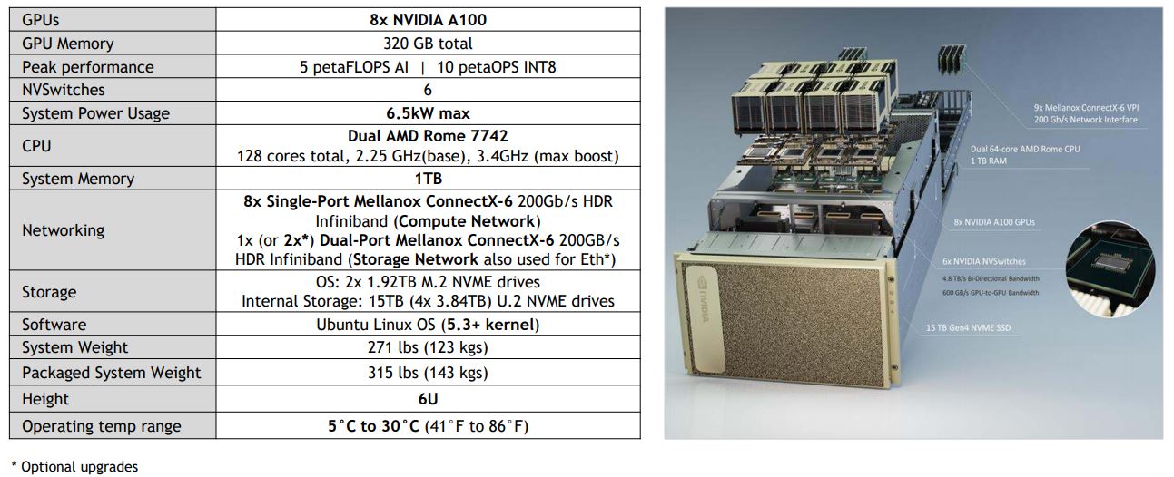
The big implications here are twofold. First, with this design, NVIDIA will effectively make its partner OEMs obsolete. NVIDIA’s plan is to package the CPU, memory, interconnect, and GPU together. NVIDIA already sells its high-end SXM4 GPUs either in the 4x GPU Redstone or the HGX boards. We showed the HGX board in our Inspur NF5488M5 Review extensively and will have more on Redstone in our Dell EMC PowerEdge XE8545 review. However, the Redstone platform made an appearance at GTC (left of this photo n the table.)
While NVIDIA has been working this way for some time, at some point once NVIDIA sells not just the GPU assembly, but also the full CPU, DRAM, and interconnect, then the only place for an OEM/ VAR to add value is in service and potentially the NVMe SSDs used (assuming non-NVMeoF storage.)
NVIDIA is previewing Grace since it is still a more conceptual design. Things may change, but it is targeted for a 2023 deployment. NVIDIA is showing how it plans to be a 3-chip company with GPU, CPU, and networking.
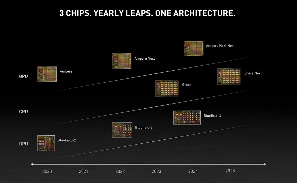
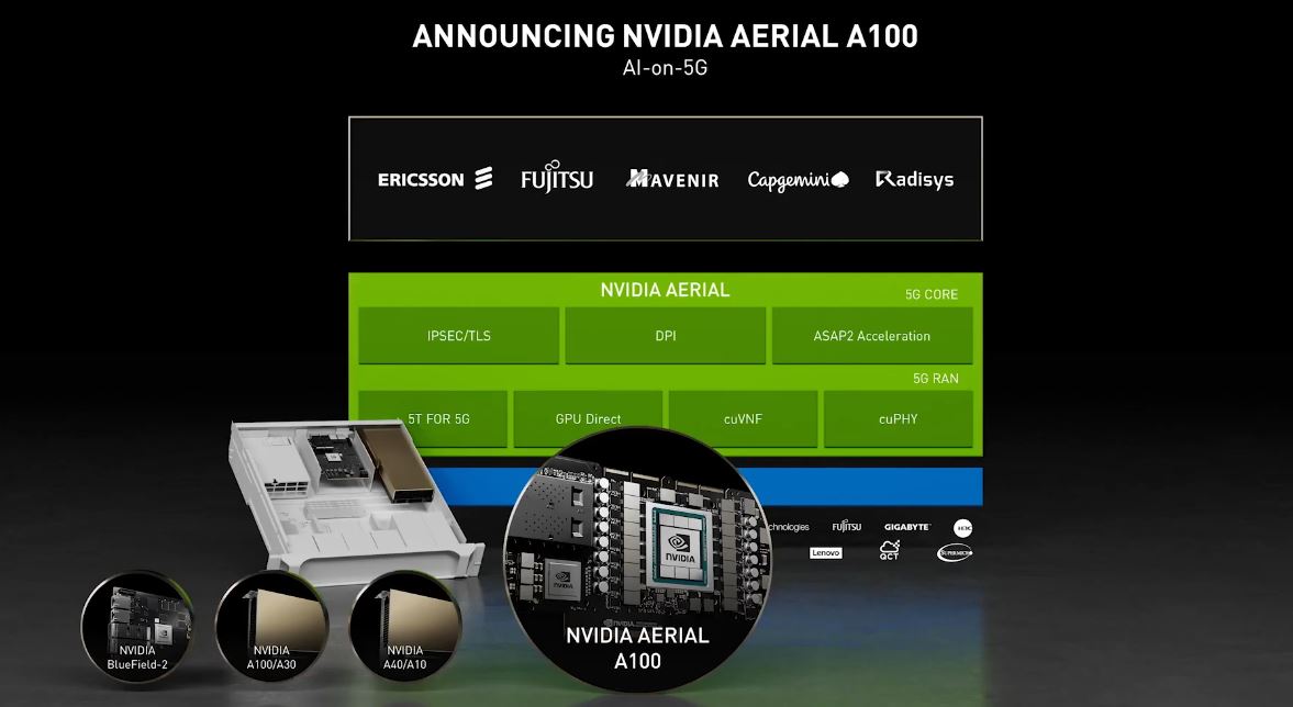
This is not just a CPU connected to a data center high-end GPU either. NVIDIA is also looking to bring Arm CPUs if even only via Bluefield, to its GPUs outside of Grace before 2023. For example, the Ariel A100 is designed for a 5G base station and items like the BlueField-3X.
Make no mistake, NVIDIA is working to free itself from being a component vendor to being a systems vendor in the era of AI and that means it is going to put increasing emphasis on its systems and software business. This is very cool, but it is also a statement to the industry that NVIDIA is looking to subjugate other players in the market soon. NVIDIA will say it values partners, but it is effectively moving to take the hardware off the table for its partners and is working on parts of the software side as well.
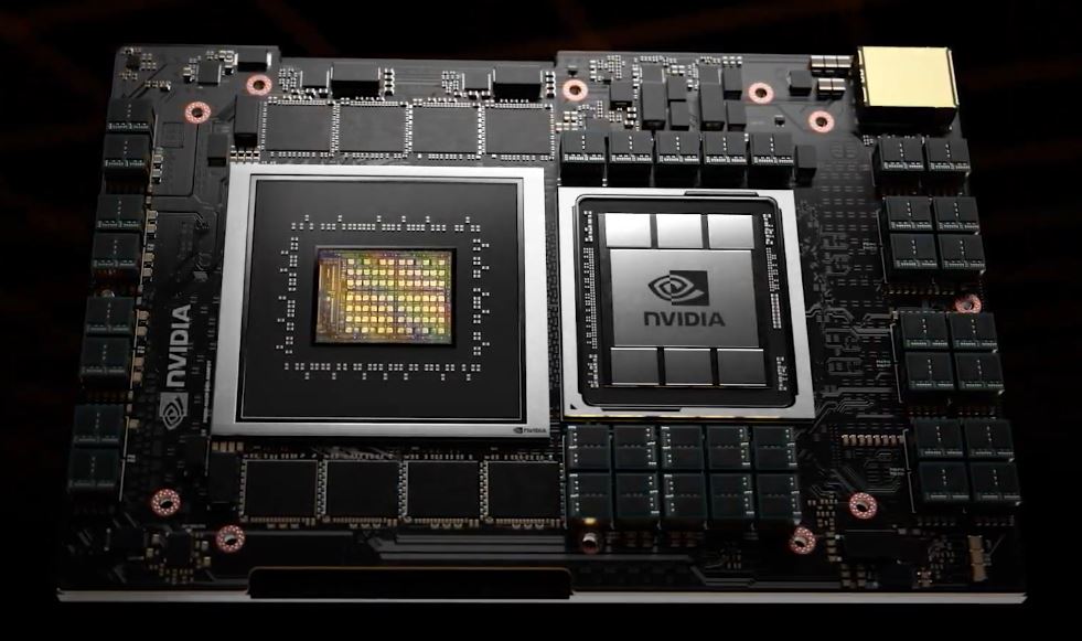
Looking at the Grace Package
Taking a look at the CPU die shot (which is likely a conceptual rendering rather than the actual chip) we can at least look at what NVIDIA is showing. Again, this is likely a rendering, but here we can see an array of seven high and twelve across or 84 elements that look like they could be cores similar to what we saw on the NVIDIA BlueField-3 rendering today. Eight look like they may be something different but we can see a well-defined pattern.
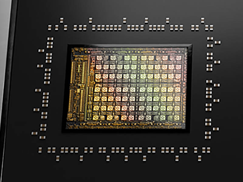
The die shot also feels light on other structures for connectivity compared to what we normally see on other CPU dies. Given how I/O heavy the Grace platform is supposed to be, this seems like this is likely a rendering so perhaps it will be best to take this as a directional rendering.
Also, when we look at the GPU, this looks more like it is an Ampere GPU than a 2022/ 2023 GPU:
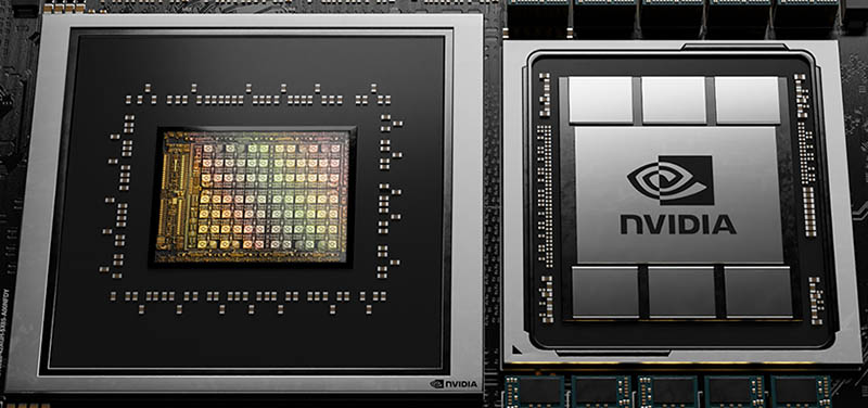
This is what NVIDIA’s 2022 competitor Intel will be packaging with Ponte Vecchio with 40+ different pieces of silicon.
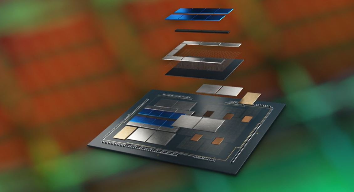
Our best guess is that what was shown as the Grace rendering is likely different from what we will see actually launched.
Important Reading the Grace Messaging Critically
At STH, we discuss how the 2022 generation of processors will be a huge leap in performance and capabilities compared to what we have in 2021. This year, the fastest CPU on the market is the AMD EPYC 7763 that has a SPECrate2017_int_base of around 800 in a dual-socket configuration or around 400/ CPU. Jensen during the keynote said that the NVIDIA DGX A100 only gets around 450. That seems very low for dual EPYC 7742’s as one can see as an example here. Perhaps Jensen was given that number, using 2019 CPUs, using older gcc versions? STH was even well over 600 from the same CPUs, and we are always lower than vendors due to how much more tuning vendors do on their platforms.
NVIDIA did not show the marketing slide it showed the press, but the number was given that NVIDIA expects:
- Over 900GB/s Cache Coherent NVLink CPU to GPU
- Over 600GB/s CPU to CPU
- Over 500GB/s LPDDR5x with ECC
- Over 300 SPECrate2017_int_base
This slide (will update if we get a non-watermarked version) says >300 we would naturally assume that if NVIDIA was targeting 400+ it would simply say that. As such, the CPU power of the 2023 chip, is expected to be about that of a top-end 2019 x86 chip or about 75% of 2021’s top-end AMD EPYC 7763. We fully expect what NVIDIA is saying its 2023 Grace’s Arm CPU complex at a >300 SPECrate2017_int_base will be less than half the performance of a top-bin x86 part in 2023.
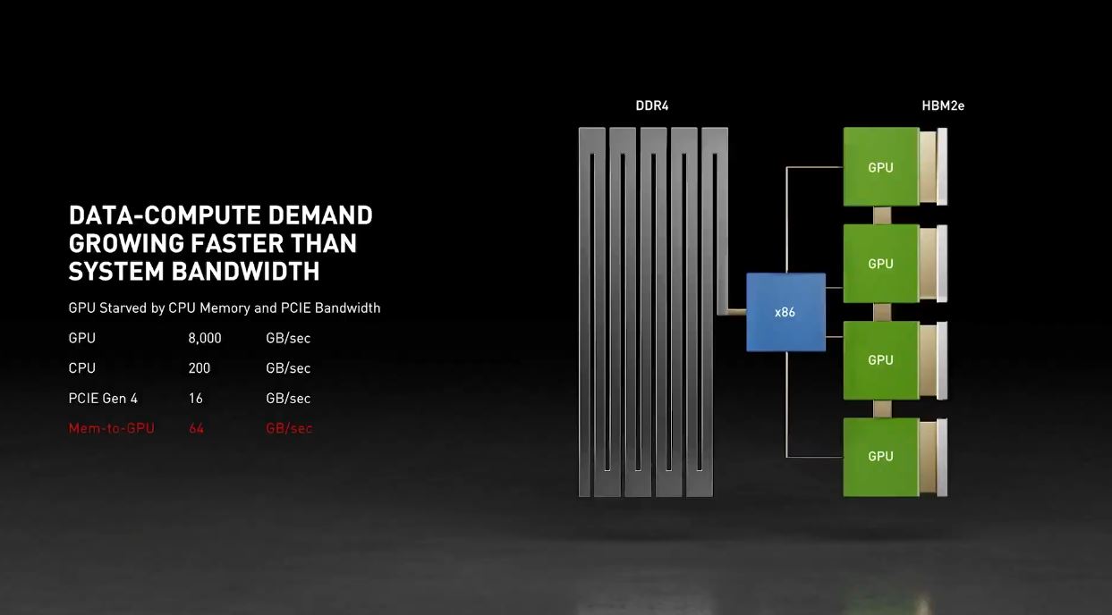
On the memory bandwidth side, NVIDIA did something that many may miss. NVIDIA is cheating a bit on PCIe bandwidth. 16GB/s would be PCIe Gen3 speed in one direction, not bi-directional bandwidth and not PCIe Gen4. Furthermore, PCIe Gen4 is twice as fast. So one could say NVIDIA’s current GPUs based on PCIe Gen4 Ampere have 32GB/s of bandwidth to the host CPU in each direction or 64GB/s bi-directional bandwidth.
Looking to early 2022, we will effectively double bandwidth from where we are today with PCIe Gen5. It makes the 500GB/s look like a big number to show 16GB/s to 500GB/s, but comparing 32GB/s or 64GB/s in today’s PCIe Gen4 terms or roughly 64GB/s or 128GB/s in the PCIe Gen5 era would be more relevant and accurate. The only reason to put the wrong figure for PCIe Gen4 performance is to make the 500GB/s look like more than a 10x jump. Even in a PCIe switch situation with the NVIDIA DGX A100 if there were two GPUs on each switch (not represented in the corresponding photo) one can get full x16 to a single device through the switch to the host CPU even if the other GPU is saturating an x16 link of bandwidth using GPUDirect_RDMA across the PCIe switch.
When simple things such as using the correct speed for a PCIe Gen4 x16 link are not done in a presentation, it should make folks nervous about how those slides were crafted. It is unlikely this is coming from Jensen but it is important. Claiming a 20x from current Gen PCIe to CPU is not correct, 10x is borderline, and in 2022 PCIe Gen5 terms the real number will be more like 4-10x to get to 500GB/s.
The other side to this is why we need eight Arm-based CPUs? In theory, NVIDIA could build a GPU die with HBM2e and LPDDR5x support and then not need the Arm CPU. Indeed, if the Arm CPU is less than half as powerful as its 2023 contemporary CPUs, then one could build systems with fewer CPUs by having more GPUs than CPUs, much as is done today. Fewer CPUs mean less power for CPUs and less interconnect power.
The difficult part is that we would not read so critically if NVIDIA did not misrepresent something as simple as PCIe Gen4 bandwidth.
A Nail for Power
A final point was a bit that Jensen said during the keynote that cannot be ignored. NVIDIA said it will continue to support x86 and Arm. What was not noted, was supporting IBM Power. NVIDIA and IBM had the largest supercomputers in the world recently, and now NVIDIA is excluding Power from its support list. That is scary for the Power side.
Final Words
Overall, the NVIDIA Grace announcement shows us a few things:
- There is an exciting new Arm + GPU compute model that NVIDIA is scaling from the high-end data center to the edge
- NVIDIA is on a path to leverage its Arm acquisition in the near-future of product announcements. We are going to see NVIDIA, Intel, and AMD all with some degree of CPU, GPU, and networking capabilities
- Every NVIDIA hardware partner should be making alternative plans now as NVIDIA Grace effectively removes the need for hardware OEMs/ VARs
- NVIDIA’s data center marketing is now fudging numbers
- IBM Power is fully on a path to relegation to upgrading legacy environments. This is a blow to IBM’s AI storyline.
- While Ampere is pushing its Altra with NVIDIA GPU today, it is going to need some major innovation to be relevant in the AI space with NVIDIA GPUs in 2023
- NVIDIA has a win with a 2023 Alps Supercomputer with HPE and CSCS, but it is touting that it is “The world’s fastest supercomputer for AI” at 20 Exaflops of AI. This seems like a stretch given it has not been delivered and NVIDIA quotes figures such as lower precision and sparsity when quoting AI performance numbers.
This is certainly a big announcement and one we hope to hear more about in the future. We also hope NVIDIA works to clean up its marketing to be less misleading. Using AI ops is a stretch, but misquoting PCIe Gen4 bandwidth to make a future product look better should never have made it to Jensen’s teleprompter, especially when one can fact-check this easily. This is a cultural issue that hopefully, NVIDIA will address.
Update 2021-04-12: I spoke with NVIDIA. Here are a few notes:
- I got confirmation that the Alps Supercomputer 20 Exaflops of AI is using FP16 sparse
- On the PCIe Gen4 16GB/s NVIDIA is using half of the unidirectional bandwidth assuming two GPUs on a PCIe switch are simultaneously saturating the x16 link. We agreed that there is a maximum single GPU of 32GB/s unidirectional bandwidth. However, with two GPUs on a PCIe Gen4 switch and a x16 uplink one gets half the bandwidth to each GPU. I still maintain this is misleadingly labeled (others have had this feedback as well and I relayed that feedback.)
- The SPECrate2017_int_base of 450 for the dual EPYC 7742’s in the DGX A100, the way they got that figure was internally using GCC as a compiler, not AOCC which would be the standard way to benchmark and present a published SPEC result. We agreed that Jensen should have said an estimated 450 SPECrate2017_int_base for the DGX A100 since that is not an official result.
- The over 900GB/s Cache Coherent NVLink CPU to GPU that NVIDIA shared is cumulative bi-directional bandwidth so there are over 450GB/s in each direction per the clarification discussion.
- NVIDIA wanted to point out it is for having a hardware ecosystem. I will just let our readers decide the direction this is going for themselves.
Update 2021-04-14: This is covered in our GTC 2021 video if you want to hear more:


They showed lots of nice things but marketing is really getting out of control in this business.
Thanks for clarifiying things. I got really curious about what “AI exaflops” mean while I watched the stream.
LPDDR5x is interesting. Can’t find specs on JEDEC website yet. Even Samsung didn’t talk about LPDDR5x. But if we assume those 8 chips have 64 D-lanes each that would make a nice frequency of ~8 Ghz to get to 512 GB/s.
I’m also curious about the DRAM capacity, especially when we look at DRAM that’s desgned for smartphones. If every LPDDR5x chip has 32 GB (that’s about 2x of today’s best LPDDR) and we have 8 chips per “Grace” (don’t think clamshell makes sense for LPDDR) and 4 “Graces”, that would make 1 TB of DRAM. Probably less than that because ECC will most likely work like on GDDR. 1 TB seems low for such a machine in 2023.
Regarding the 16GB/s PCIe Gen4 business.
NVIDIA has been consistent that when they discuss systems they really only mean their current top end DGX system. So while a single GPU *can* get 32GB/s that’s not a use case they ever talk about. Generally all GPUs will need to be reading at the same rate which means the 16GB/s is a real number for NVIDIA DGX systems.
So I wouldn’t say it’s misleading, just that their marketing is heavily influenced by the DGX team.
They’re taking a system with NVMe storage, NIC, and GPUs off of NVMe switches, then quadrupling the number of CPUs in a system?
And @wes you can use DGX and do a container/ VM per GPU right? It may not be the only use case or the dominant one, but it is a valid use case.
It’s like NVIDIA re-architected a system and says oh the new one is so much better but it’s like 34% better because of the Arm NVLink integration, 33% better from more CPUs and better architecture, 33% better from time.
I’d agree with this article. It’s cringe what NVIDIA is doing nowadays.
I don’t doubt that NVidia will have an excellent (standalone) GPU a few years from now.
But with this device they’ll be competing with CXL and PCIe 6 on the interconnection side, unless AMD and Intel decide to re-enter the APU era; and use their own proprietary interconnect.
The ARM server CPU uses less power and is more efficient, but its instruction set and clock doesn’t match the competitors; though their price for 80 cores (and threads) doesn’t compete with AMD’s high core count CPUs.
If the price that the customer would have to pay for the ARM CPU portion of that fell it might not be so bad, but a true mashup would be better than seperate chips and boost the capabilities and interconnect to a much higher level.
Reinventing the APU with a lower performing CPU than what the competition could use isn’t going to be a win – and we’ve yet to see what Intel’s GPU will offer a few years from now.
Uhhhhhhhhhhhhhhh, they’re adding 8 CPUs to get more memory bandwidth or 1 CPU per GPU.
NVIDIA $$$. Good call-out on the BS Marketing. Rob it right, you should have used PCIe G6 for 2023 competition. At 128/256GB per x16 NVIDIA has maybe more speed but requires way more CPUs.
Really good analysis.
I feel like there is gonna be quite a few more complaints from ARM licensees reaching the heard of the regulators….
As for competitiveness, it doesn’t seem like they will be further ahead than AMD at that point: MI300 will probably use PCIe 5 (maybe 6), in x32 (hence why 4 GPUs per CPU), which gives 250GB/s (or 512GB/s if pcie6) up+down per gpu.
4 GPUs per CPU gives you 1TB/s bandwidth (2TB/s if pcie6) which is the same as Nvidia.
Not sure if it’s gonna be multi socket though on AMD’s side.
If AMD has HBM on the CPU, that’s gonna be much more benadwifth, maybe less capacity though.
At least there’s 1 site that’s reading and evaluating not just reposting NVIDIA’s PR. It’s a good platform, but this article makes great points
Raptor lake in 2022 SUPPOSEDLY supports lpddr5x according to leaked slides. It looks kinda like lpddr5x, in that it’ll attain higher densities along with far greater frequency. But it won’t be a thing for a while. Also 500GB/s of CPU bandwidth?! That’s at the very least a 512bit lpddr5x memory interface
Do’h , meant to say ‘it looks like a successor to lpddr4x ‘
Thank you STH for looking critically at this.
Comments are closed.